# VDC-II
## Description
In a perfect world, this project intends to implement a clone of the Commodore
8568 Video Display Controller (VDC) chip, which is the chip that provided the
Commodore 128's 80-column text and 640 pixel graphics capabilities. While the
VDC was intended to be used primarily with display devices operating at NTSC
frequencies and which relied on interlace for high resolution displays, the
VDC-II targets instead VGA and progressive-scanned devices. 100% software
compatibility is NOT guaranteed, but I'll strive for compatibility to the
greatest extent I know how. It is written using the M-Labs nMigen hardware
description software.
## VDC-II Data Book
VDC-II Data Book
## Logs (transcription from Hackaday still in progress)
Font Editor Code Coming Along
08/01/2021 at 02:27
Besides working my buns off at my day-job, I've been slowly making progress
on a font editor application for the VDC-II core. And, by slowly, I
literally mean spending about two hours every month or so on it. Still,
progress is being made, and I'd like to toot my own horn for a moment.
The screenshot below is a current image of what the program looks like. As
indicated before, this program is written for the Z80 processor, and runs
under CP/M 2.2 or compatible operating system. Right now, this software is
optimized for the Commodore 128 and its VDC chip; however, it is quite easy
to adjust it to run on the RC2014 with a VDC-II card.
As you can see, its user interface and overall functionality is coming along
quite nicely.
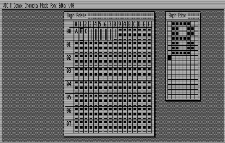 As I type this, there are still some bugs to be worked out. While editing
the fat-bits view of a character, the display gets corrupted for some reason.
I'm still trying to work out why this is. However, it does not crash the
software, and it legitimately does update the correct glyph bits, which you
can confirm by dismissing the Glyph Editor and re-opening it.
Also missing is the ability to load or save data from/to a file. This will
be coming soon enough. I'd like to get the basic program functionality
working first.
Anyway, just a reminder that I'm not dismissing this project; my professional
obligations have been taking more than a fair amount of my bandwidth. I
can't wait to be able to run this software on real hardware though!!
Work, work, work, ...
06/13/2021 at 19:43
What happened?
Well, I got a full-time job for a major manufacturer of mass media storage,
so that's been occupying most of my time.
Finally heard from Crowd Supply about a month ago that they're still waiting
for parts to complete my order for TinyFPGA BX modules. Who knew the
semiconductor shortage would take out the BX-Plorer project?
Still, I've not had two seconds to rub together to hack on the VDC-II HDL
code. Which sucks, because I am itching to make some progress with it. I
desperately want to finish it by end of this year, so I can move on to other
things.
But, now that I'm starting to get into a routine at my day-gig job, I'm
hoping to re-allocate some weekend time to get back to work on the Font
Editor code for the VDC(-II), and subsequently to that, to actually finish
the VDC-II itself. I would love to be able to get CP/M running natively on
it using my RC2014.
Adulting is hard. Avoid becoming an adult if you can.
VGA PMod Adapters
01/14/2021 at 00:53
I ordered some VGA PMod adapters from Digilent last week, and I'm happy to
say that they fit perfectly. The mechanical connection is very solid, far
better than any card edge connector I've used. Near as I can tell, the
electrical connection also seems to be good as well.
I haven't had the chance to reprogram the FPGA design to use this particular
adapter yet. I will update with my results upon completing that.
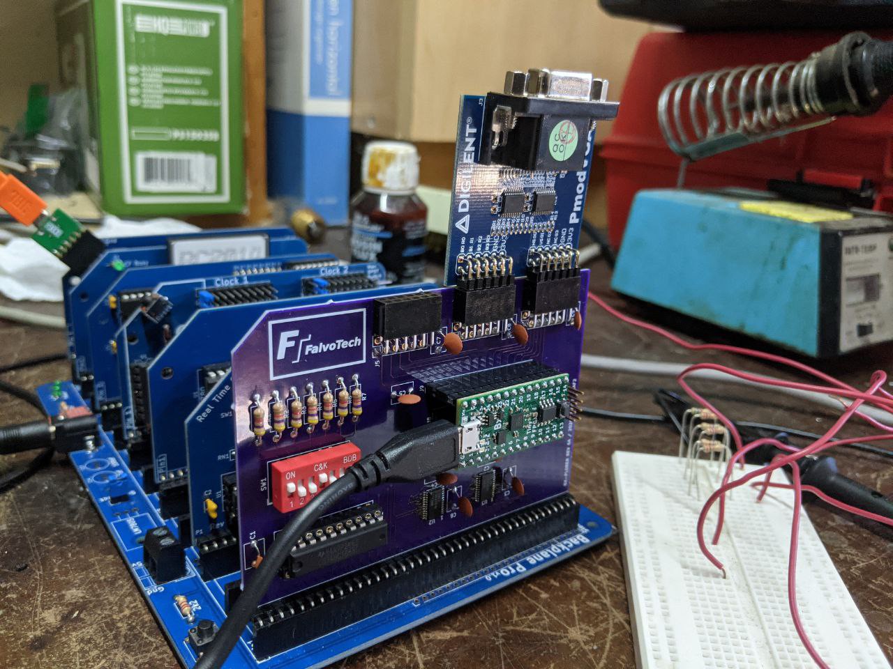 The only thing which sticks out to me, besides the height of the connector,
is ... the height of the connector. And, its orientation. But, if you can
strain-relief the monitor's cable appropriately, it should not pose a problem
for the BX-Plorer.
(Aside: my experience with how well this PMod fits into the sockets on the
BX-Plorer has convinced me that the right way forward for the Kestrel-3's
backplane should be 2x40-pin RC80-compatible connectors.)
Crowd Supply, More Parts on Order, Etc.
01/09/2021 at 21:42
Now that I have what I believe to be a functioning prototype of the BX-Plorer
design, I have reached out to Crowd Supply to see if they think this project
is worthy of crowd-funding and selling through their website. So far, after
about a week of waiting, I have not heard anything back from them. Their
website does not provide any indication of how long I should have to wait for
an answer. I've opened a support ticket with C/S as well, but again, no
response. If C/S doesn't respond within another week or so, I shall start
looking into selling my kits elsewhere.
In the mean time, I have placed an order for three Digilent PMod VGA adapters.
(Three, because these things are easy to lose!) Although these adapters
support 4 bits per gun (and, thus, support 4096 colors maximum), I can only
use 3 at the moment because of my previous wiring mistake. Still, it should
work for the purposes of demonstration.
Another thing I'd really love to hear back from C/S about is my outstanding
order for five more TinyFPGA BX modules. Back in December, they said that
they expect a new shipping date some time in January. I sure hope they
haven't forgotten about me. I'll give them until February before I contact
them again about my order.
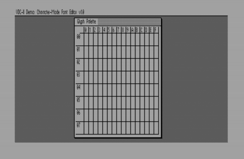
While waiting for all this stuff to work itself out, I've been making
progress on the font editor demo. Here's the latest screenshot (taken off a
Commodore 128 emulator), and is a good representation of what it should look
like on an RC2014 with a VDC-II card as well. I still need to write the code
to render all the characters inside the table cells, to scroll the glyph
palette table up and down as appropriate (to allow selecting any of the 512
supported characters), and of course, the actual editor interface as well.
Still, progress is progress.
 Revision 6A boards here; work great.
01/02/2021 at 07:31
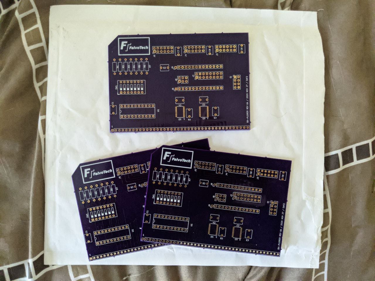
Just before Christmas, I received the three prototype boards for revision 6A
from OSH. The boards look great, but I wasn't able to construct one until
yesterday evening.
 Assembly went ... not quite as smoothly as I'd've liked for the first board I
tried. It was a bit colder in the garage than I'd've liked, but the solder
hated it more than I did. While attempting to drag-solder the 74LVC8T245PWR
chips onto the board, no matter how much solder I used to flood the pins, it
refused to make a clean solder joint. Wicking the solder just wasn't working
well, so I tried to apply a bit more pressure. While that worked to get the
solder hot enough to wick, it also bent the pins of the chips, and ... yeah.
Lesson learned: do not drag-solder when your workspace is cold.
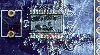 (note the red lines showing where the pins got crushed together.)
After refining my technique to use tack-soldering instead, and making sure to
wick excess solder pulling away from the chip instead of trying to sop all
the excess in one fell swoop by dragging the wick across the pins,
construction went relatively smoothly. I completed the build of the 2nd
prototype card in about six hours.
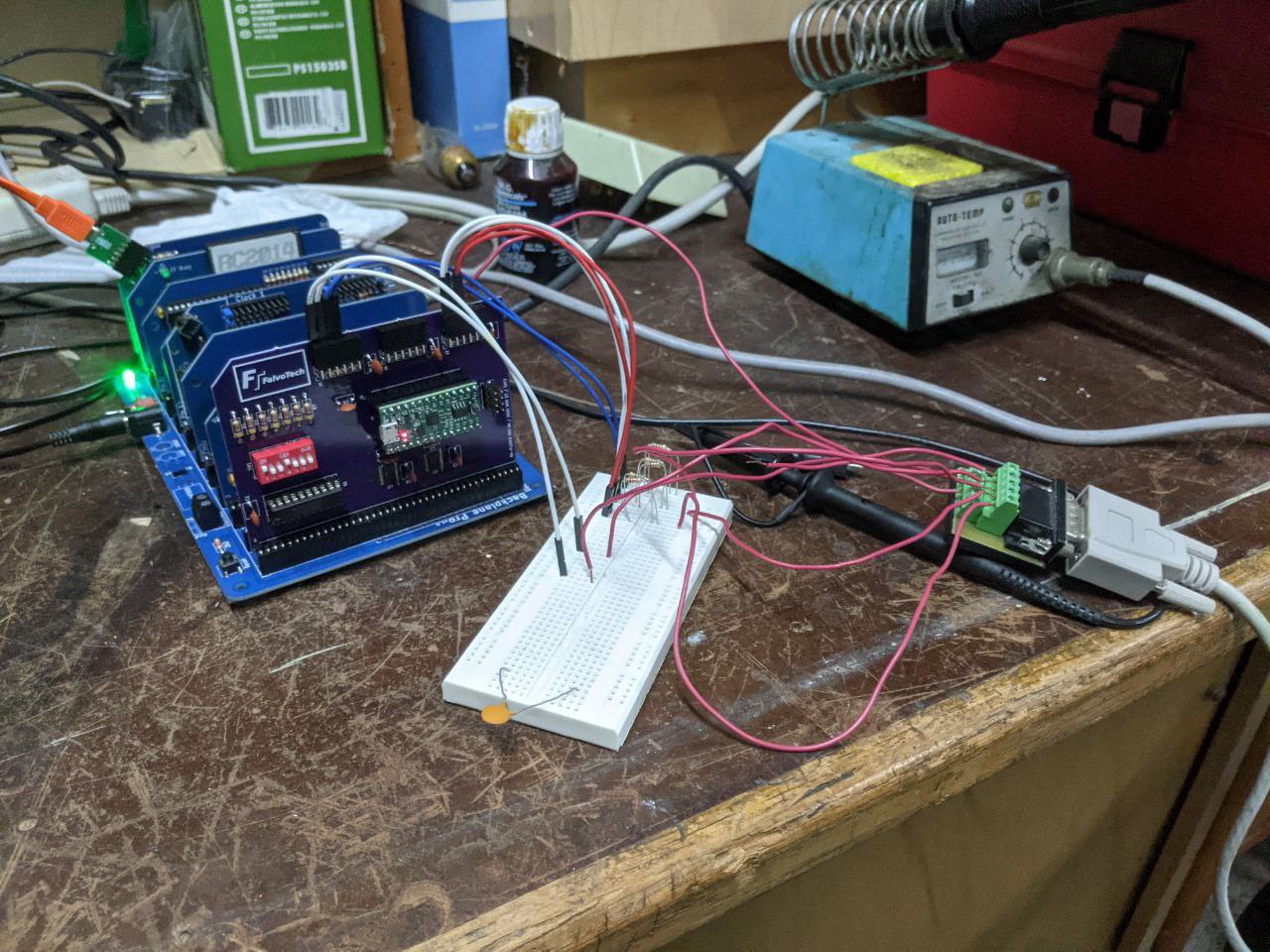
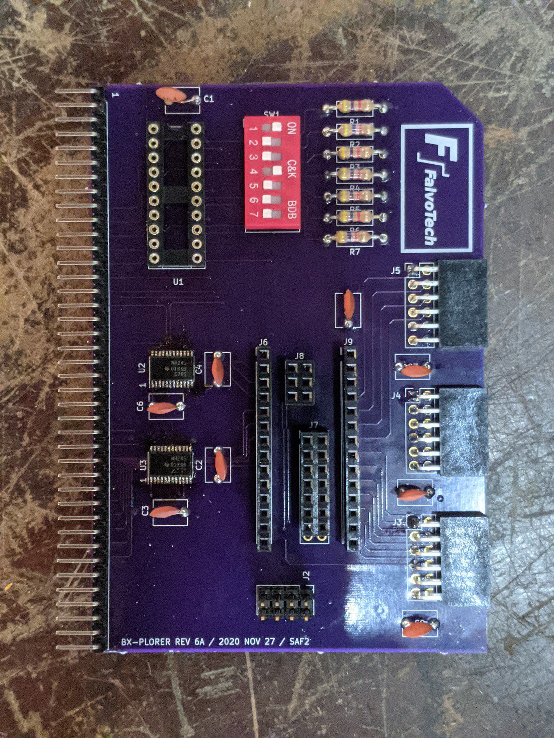 After fitting a TinyFPGA BX module to the card, I was able to use it as a
proper VDC-II card by routing wires over to a breadboard with a resistive DAC
on it.
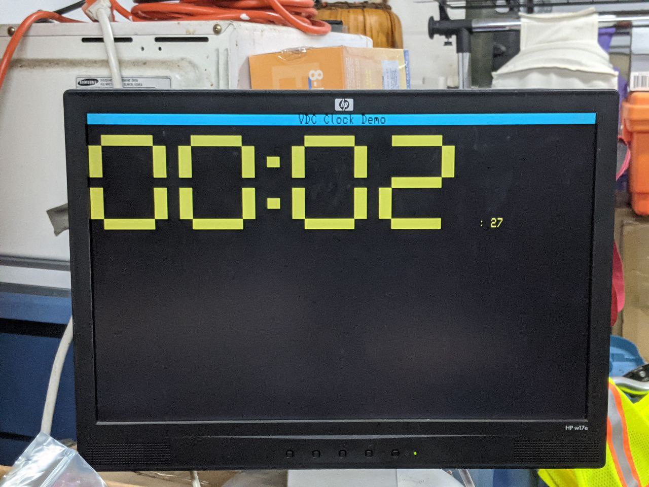
 I ran the old clock demo I'd written some time ago, and it runs perfectly.
(A more advanced demonstration which puts the VDC-II into bitmapped graphics
mode is still under development as I write this.)
 Next steps include:
* Double-check and make sure the extra I/Os exposed by the new Rev 6A board
have continuity. If they do not, it'll be because of how I soldered the
connectors to the bottom of the TinyFPGA BX module, and not due to a wiring
issue on the 6A board. (I already checked the latter, and they seem to work
as far as I could tell.)
* Begin the process of seeking Crowd Supply feedback.
* Continue working on the VDC-II font editor tool. I've neglected to post
updates here mainly because I never seem to make big enough progress with it;
that, and I'm coding it on a Commodore 128 emulator for convenience. But, I
suppose I will start posting software updates here too, as eventually, this
software will be ported over to the RC2014. The VDC and VDC-II parts will
need somewhat different initialization logic, but once initialized, they
should behave identically. So, having the C128 version handy as a reference
implementation will be useful.
Notes on How To Solder Belly Connectors
12/03/2020 at 18:43
I have been thinking about how to reliably solder the surface-mount pin
headers to the TinyFPGA BX module for some time now. I think I've come
across a solution.
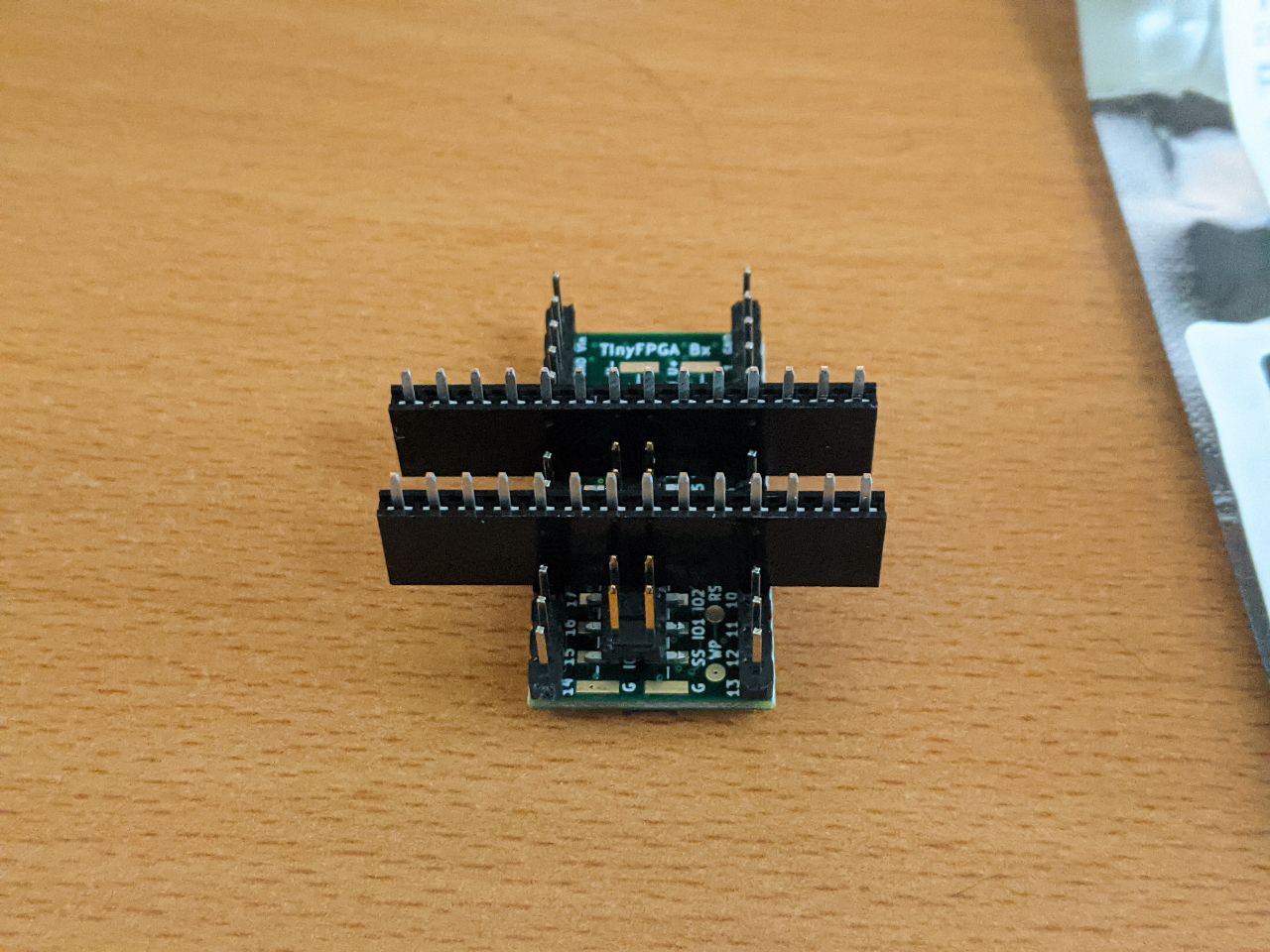
1. Solder on the 14-pin outer/through-hole connectors. It's important that
they be soldered for mechanical stability in later steps.
2. Insert two pins of the surface-mount pin header into female strip socket.
3. Insert the female strip socket cross-wise on the TinyFPGA's through-hole
pins.
4. Insert another strip socket a few pins away to lock in the registration.
5. Now you can solder the ends of the surface-mount connector to the board
with full confidence that they'll line up correctly with the socket on the
PCB.
6. Scoot the cross-wise sockets down, and solder the other end of the surface
mount socket.
7. Now you can remove the cross-wise sockets, and solder the remaining pins.
Here's a picture of a mock-up which demonstrates what the arrangement should
look like after step 4, but before the completion of step 5.
 Demo Software Project: Font Editor
12/03/2020 at 18:31
It has occurred to me that my plans to complete VDC-Forth are essentially
kaput; it is a user interface model for a Forth that I'd hoped would give me
some unique insights and inspirations, and instead I have essentially coded
myself into a corner with it. While I do intend on playing more with the code
in the future, it's not clear to me that it will remain my "go-to" piece of
software I can point someone to and say, "Look, here's code that works directly
with the VDC-II core you can study."
One thing that I will need in the future, though, is a font editor for this
module. So, I figured, why not write a font editor for it, using it? And, so,
that's what I'm doing.
It's written to use 640x200 bitmapped mode, monochrome. I chose this because
had I used text-mode, I couldn't easily alter the font heights. Remember that
the VDC chip supports fonts as small as 1 pixel tall and as tall as 32 pixels.
Since vertical sync timing is dependent on this height, every time I'd need to
alter the font height, I'd need to recompute (dynamically) the CRTC settings.
With this comes the risk of user-visible loss of monitor sync, which is
annoying to say the least.
So, bitmapped mode it is. So far, I've implemented code to draw horizontal
lines and draw filled rectangles using patterns. Although their APIs are quite
primitive and low-level, they work.
Just ... not very fast. I predict the issue is caused by needing to read from
and write to the VDC for every byte transferred. I could probably double
performance by only read-modify-writing the left- and right-hand edges of the
rectangles, and just blindly writing the interior bytes.
Even so, this software isn't intended to win any races, and certainly not to
race the beam in any way. So, correctness is the most important aspect of the
code. I might spend some time to optimize the code a bit, but I won't spend
too much time on it.
Now that I can draw nice rectangles and horizontal lines, the obvious next step
is vertical lines and, after that, text. Once that's done, I'll have the
ability to render the complete user interface for the font editor. From there,
actually implementing the editor proper should be relatively simple.
I think.
Source of Error Found
11/27/2020 at 23:38
So, why did I make such an egregious error when designing revision 5B boards?
Because the TinyFPGA BX project has (or, at least at one time, had) poor
revision control and misleading or missing documentation.
When I was building revision 5B, I was working off of this photograph, which is
one of the only documented listings of the I/O pins accessible on the underside
of the TinyFPGA BX module. (If you can find an official description of those
connectors on the https://tinyfpga.com website, please send me the link!)
Observe the bottom "belly connector" (what do you call those things anyway?) is
a 2x7 surface mount connector, which lines up with what I've built the 5B to
work with.
However, if you look at the current OSH Park PCB artwork, you'll see that
there's a 2x8 surface mount connector in its place. This matches up with the
actual hardware I tried using to build the latest prototypes with. As far as I
can tell, it looks like the exact same pin-out as the 2x7 connection, but with
an extra pair of ground pins.
Of course, looking at the schematic, I see that it describes the 2x8 connector;
but, considering the Crowd Supply updates are newer than the schematic up on
Github and showed the 2x7 connector, I didn't put much stock in trusting it.
Turns out, Crowd Supply's information is outdated. And, strangely, I can't
even find reference to the 2x7 connector in Github's history, suggesting that
the CS campaign started before the Github repo even existed.
So, yeah, I learned a lesson on this one: never trust the updates on Crowd
Supply. Even if newer than repository documents, they may not reflect current
reality.
OK, back to hacking on the next PCB revision.
Revision 5B PCBs are trash; need another revision.
11/15/2020 at 23:19
Rev 5B boards have a critical design failure. The "belly connectors" of the
TinyFPGA BX module has two parts: one is a 2x3 surface mount pin header, and
the other is a 2x8 surface-mount pin header. You can use a 2x7 pin header for
that connector; but it must be offset by 100mil in order to work.
Problem is, if you look at the PCB artwork, you'll see that the 2x8 belly
connector has only 14 pins. And, it's not offset. Which means that the whole
design is junk.
There are no work-arounds for this. I need to spin a new batch of PCBs with a
proper 2x8 belly connector. Sigh.
Upon inspection of the rest of the PCBs, though, everything else looks nice.
I'm particularly pleased with the host Pmod connector alignment. So, there is
that, at least.
Dammit, I really am getting impatient with this project, though. I'm spending
too much time waiting and burning through way too much cash.
Revision 5B Boards Completed
10/17/2020 at 22:10
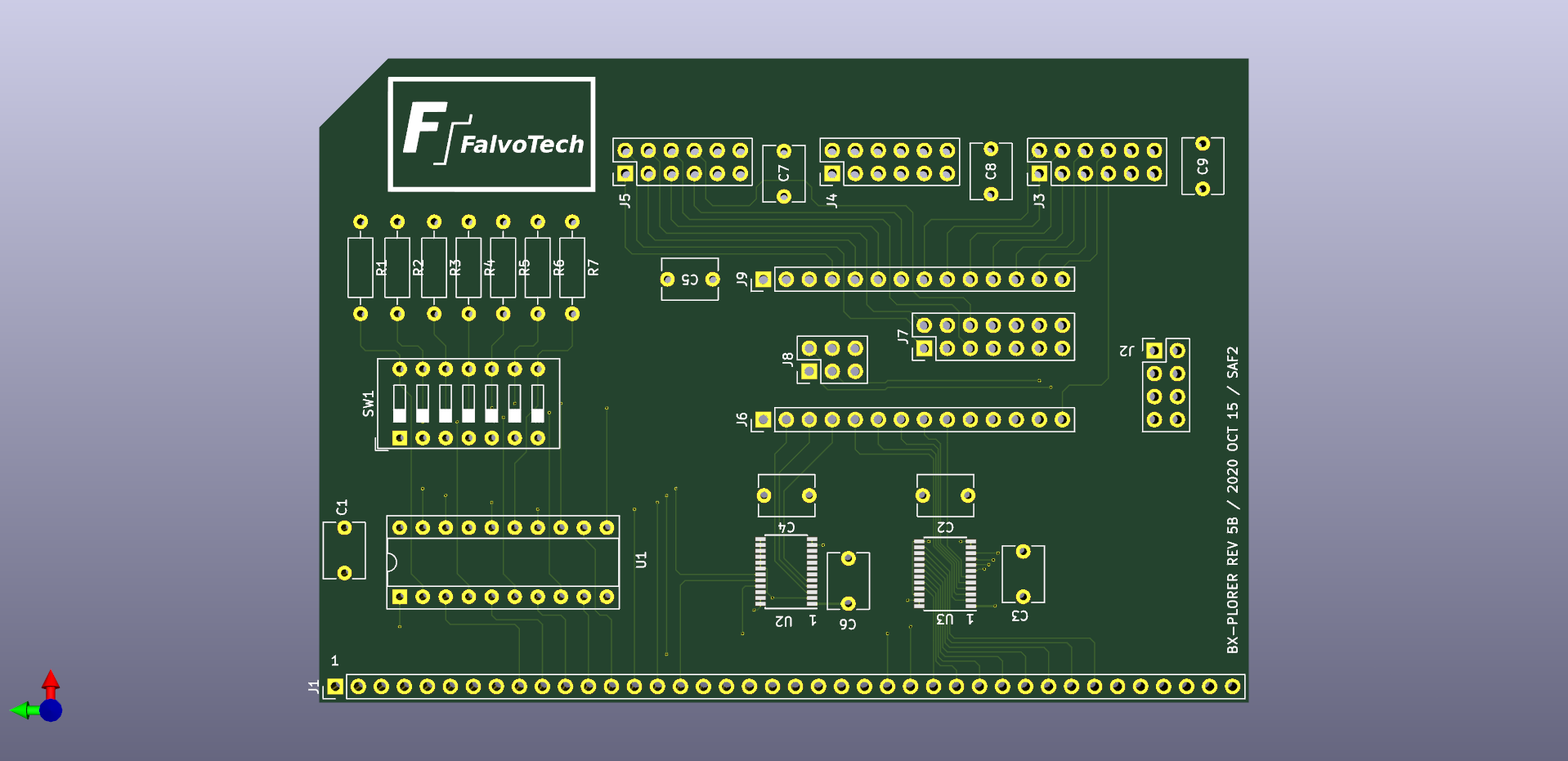
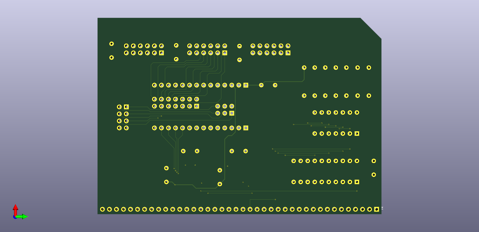
I'm happy to report that I've completed work on yet another revision of the
BX-Plorer PCB, and this one even includes a logo and more prominently placed
revision and release date. Yay for professionalism!
Even more than that, I've managed to source the proper connectors to support
honest to goodness Digilent-compatible Pmod host ports! This allows a wide
variety of pre-existing Pmod-compatible attachments to be used with your
RC2014.
Test cards have been ordered from OSH Park. They should arrive in a few weeks.
I still need to place the orders for the rest of the components though. I
should be doing that later this-coming week.
 BX-Plorer: Meet the New Card, Same as the Old Card
10/08/2020 at 20:11
As this project evolves, I'm noticing a distinct yet synergistic
compartmentalization in the roles and responsibilities of different project
components. When I started this VDC-II project, I'd just been convinced by
interested members of the community of the value of developing Kestrel-3
computer parts for the RC2014 backplane. I later observed that my RC2014 Zed's
flash BIOS image could be built with Commodore VDC support, and after reading
up on that chip's technical specs, I realized that it was a fairly close match
to what I'd wanted to achieve with my own CGIA concept. So, rather than
re-inventing the video support with the CGIA, I figured I'd just piggy-back
what was already there, and decided to reimplement the VDC. This benefits both
RC2014 and Kestrel-3 communities, since any Kestrel-specific enhancements I
make to the design later on can benefit both communities, not just the one.
So, I set out to just develop a (mostly but not completely compatible) clone of
the Commodore 8563 VDC as used in the Commodore 128, using affordably priced,
off the shelf FPGA development boards. That became the VDC-II project you're
reading about now.
I've always intended to release this project as a kit of some kind, so that
RC2014 owners can, in long-standing RC2014 community tradition, build their own
video card. That means, as part of the kit, they'd receive the PCB, all the
chips, a pre-programmed TinyFPGA BX module, and other miscellaneous parts
needed to have a working video card.
However, I now realize that the very circuit I used to interface my TinyFPGA BX
module to the RC2014 backplane is itself useful as a self-standing product in
its own right. You could see a less developed realization of this, more or
less explicitly, in previous log entries where I first mention breaking up the
FPGA part of the circuit from a mezzanine card containing the analog VGA
circuit.
Going forward, I've decided to formalize the separation of the FPGA project
card from its applications. First, the FPGA project card now has an official
name: BX-Plorer. It lets the consumer of the card explore FPGA designs using
the TinyFPGA BX module.
Second, I've decided to factor the BX-Plorer out into a separate git
repository. I'll update my Hackaday.io configuration accordingly shortly after
making this post. This implies that, Coming Soon, there'll be a separate Git
repository for the VDC-II design files and the software stack needed to drive
it. I'll (re)post updated links in a separate log when everything is in place.
Related to the first two points above, for now, both BX-Plorer and VDC-II
updates will happen in this Hackaday.io project. As I write this, I have no
plans of factoring the two projects out here. These two projects have been
co-developed from the get-go, and I don't see that changing any time soon.
Third, what of the VDC-II-based RC2014 "video card"? Is that now dead? As I'd
originally conceived it, yes. With all the other video card projects that
people are concurrently producing for the RC2014 (link 1, link 2, link 3), it's
not clear to me how I can compete for mindshare. However, if there's enough
feedback, I can see offering a BX-Plorer Cost Reduced/Fixed Function card as a
dedicated video card. If this is something that is still desirable to readers,
please do get in touch to let me know.
(Besides, you can always use a regular BX-Plorer with a pre-programmed TinyFPGA
BX and analog VGA mezzanine still.)
Fourth, this does not affect the development of the VDC-II itself. I still
need a video card, for both my RC2014 and for my own future homebrew computer
design. The VDC-II project is not dead.
When, not if, you see these new terms being bandied about in my project
updates, now you'll know why and where they come from. :) Until next time!
Revision 5 Circuit Design Underway
10/08/2020 at 18:05
As I continue to read up on my responsibilities for working with Crowd Supply
(CS), I realize that, being a vetted interaction process, CS is almost
certainly going to call me out for not exposing all of TinyFPGA BX's I/Os. So,
I'm going to head that issue off now and work to expose all of the I/Os that
this module has to offer. This will in effect turn the card into a generic
FPGA development card. I'll mention more about this in a related but separate
project log update.
This is not as simple of a task as it sounds; I need to:
* create a new TinyFPGA BX schematic symbol.
* create a new TinyFPGA BX footprint for PCB layout.
* figure out how to expose all the I/Os.
* create revised schematics and PCB layout.
These steps took me about three days so far, and I'm still working to complete
the list. Here's a summary of the changes I've made to the design so far and
what can be expected from revision 5A boards.
First, the dedicated 2x7 pin socket that I'd intended to replace the 14-pin DIP
socket (in an unreleased revision 4B PCB design; you can see it in the Github
repo though) has been replaced by a set of three 2x6 pin sockets, spaced 0.9"
apart, and whose pinouts comply with Digilent's Pmod interface specifications
at 3.3V. I'm currently placing them across the top of the PCB for easy access,
as that's the only edge long enough to accommodate them. This brings 24 I/Os
out for general purpose use. There's a catch, though; these sockets are not
right-angle sockets. I intend these sockets to be used with Digilent's
12-conductor Pmod cables to attach devices to. The PCB is already big enough
to flop around in the RC2014's single row backplane socket, so you don't want
to put too big of a load on those sockets. Building a mezzanine card will
extend the height of the PCB, which will make it more floppy and less
mechanically sound than it already is. Cables can be routed, which enables
them to also act as strain reliefs. That said, if I can source through-hole,
right-angle connectors, they should be drop-in compatible, if you can find a
way to mechanically secure the contraption.
Second, I will bring out the 5 shared I/O pins to a 2x3 pin header. This
header will have a comparable pin-out to the TinyFPGA BX pin cluster. Being
that these will be exposed pins, you can connect to them using Dupont
connectors.
Between these two changes, the BX's remaining 29 I/O pins will be fully and
much more easily accessible to hardware hackers.
Revision 4A PCB Built, Works
09/24/2020 at 22:23
Just wanted to say that I finally completed building the revision 4A board;
most of the hardware was discussed in the previous log entry, but I've fitted
the '688 comparator for address decoding as well as the TinyFPGA BX module.
The result is shown in the pictures below.
I'm happy that, despite needing one bodge wire from U2 to +3.3V, it is
otherwise fully capable of working from the POV of software development.
I've already made the changes to the design files to support revision 4B, which
fixes all the known hardware bugs. Additionally, the nMigen files for the
VDC-II has been configured to output 9-bit video, so all 11 output I/Os are
known to work.
Besides getting revision 4B out the door, all that remains is a set of
mezzanine boards: one for VGA, and one for PS/2 keyboard and mouse. That,
combined with a reasonable GEOS-like GUI system, should be sufficient to make
the RC2014 into a reasonably usable homebrew computer system.
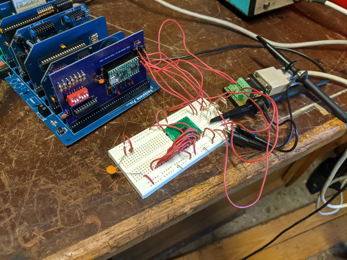 PCBs Received, First Build
09/18/2020 at 17:25
On the 14th, I received my printed circuit boards for the Pixel Pusher. Yesterday, I got around to trying to build one of the three prototype boards I received.
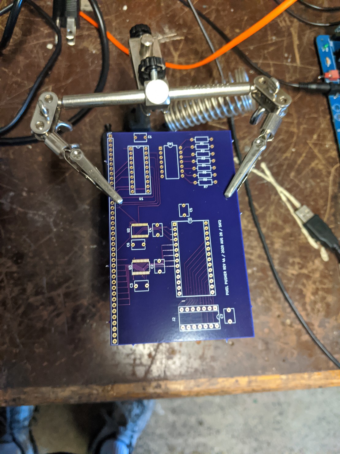 This is what a bare board looks like, component side up.
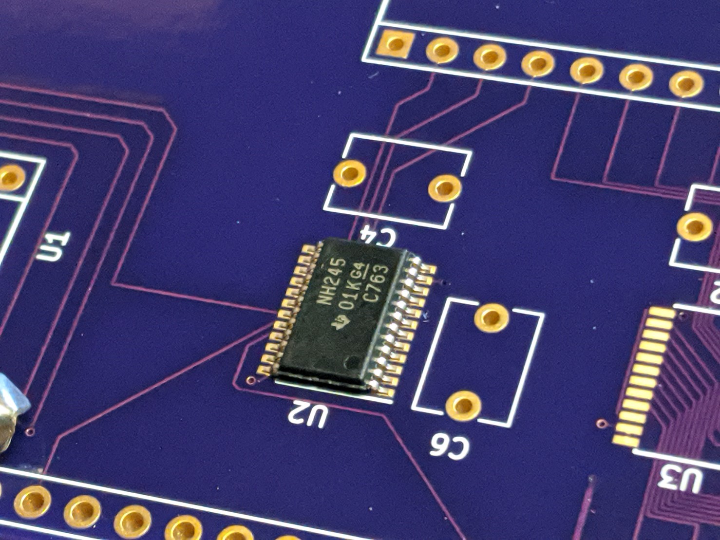 My first task is to place the highest risk components first, so as to just get them out of the way. In this case, the two 74LV8C245PWR chips, as they're incredibly small devices that even an idle breeze can cause to slip off and never be found again.
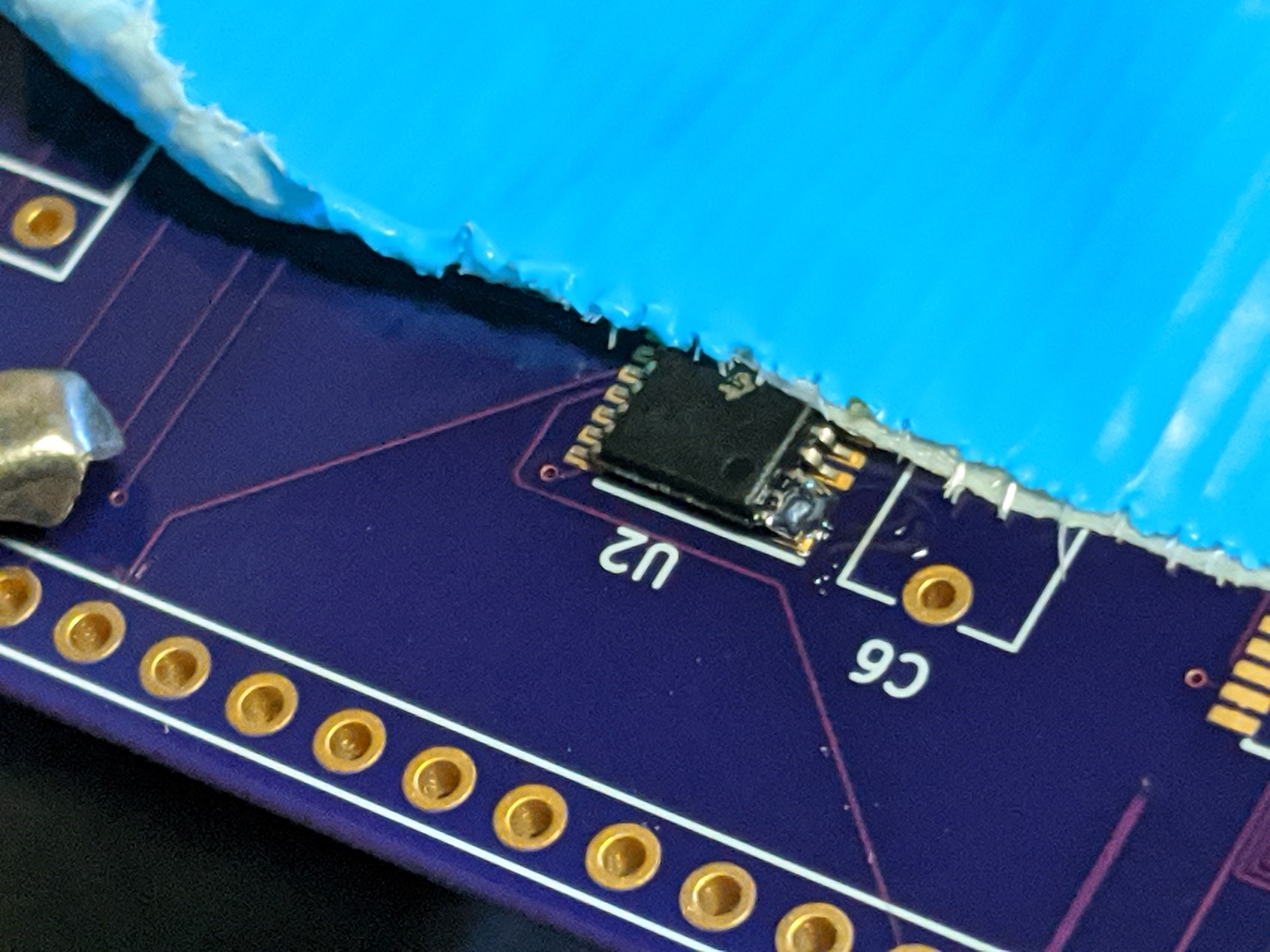 I use blue duct tape for this purpose which is not the best thing to use but it's all I had available. Tacking one corner of the chip down is sufficient to hold it in place.
PRO TIP: The ideal tape for this would have been blue painter's tape. In order to reduce the stickiness of the duct tape down to something comparable to painter's tape, I just applied and removed the duct tape strip off the work bench several times until I was comfortable with the strength of the remaining glue. The workbench was naturally dusty, so each application added more dust to the strip, which had the effect of reducing how sticky the strip was.
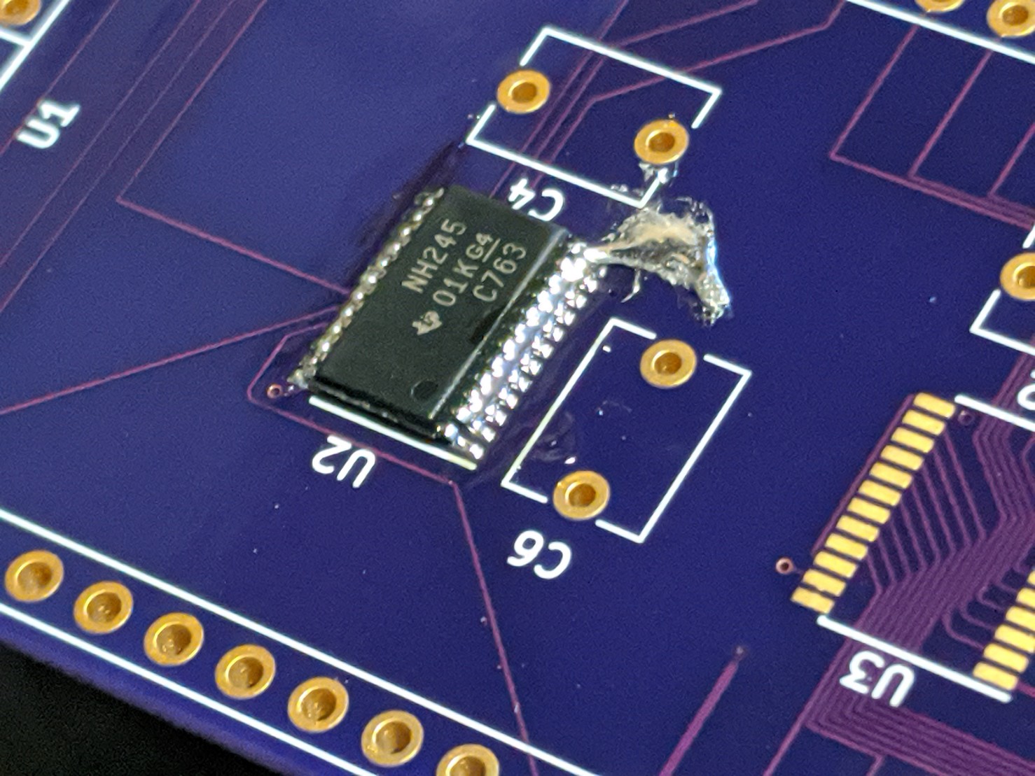 I next applied liberal amounts of solder to the chip's connections. This
ensured all pins were soldered to the pads, but it also ensured that all pins
were soldered to each other as well. This excess solder had to be removed. I
used solder wick for this purpose.
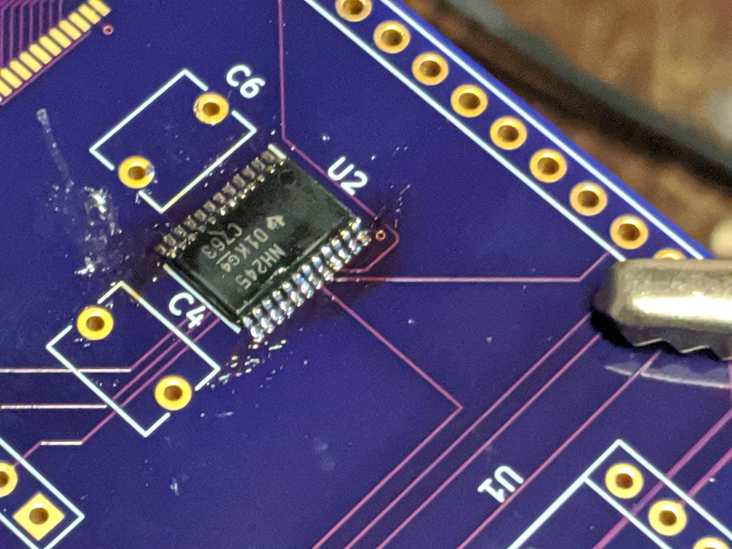 After fighting a bit with the solder wick (as evidenced by the slightly
scorched flux residue), I sopped up all of the excess solder. Solder wick does
not remove everything, and it happens to work out that what remains is
sufficient to both hold the chip in place and to ensure good contact.
Because the contacts are so small, however, It is best to perform continuity
checks with other parts of the circuit. If you need to desolder and
resolder/reflow the contacts on these parts, now is the time to do it before
other components are added.
I just discovered that the 3.3V supply pin of U2 is not connected to the 3.3V
trace. I forgot to place a via! I'll need to add a bodge wire later.
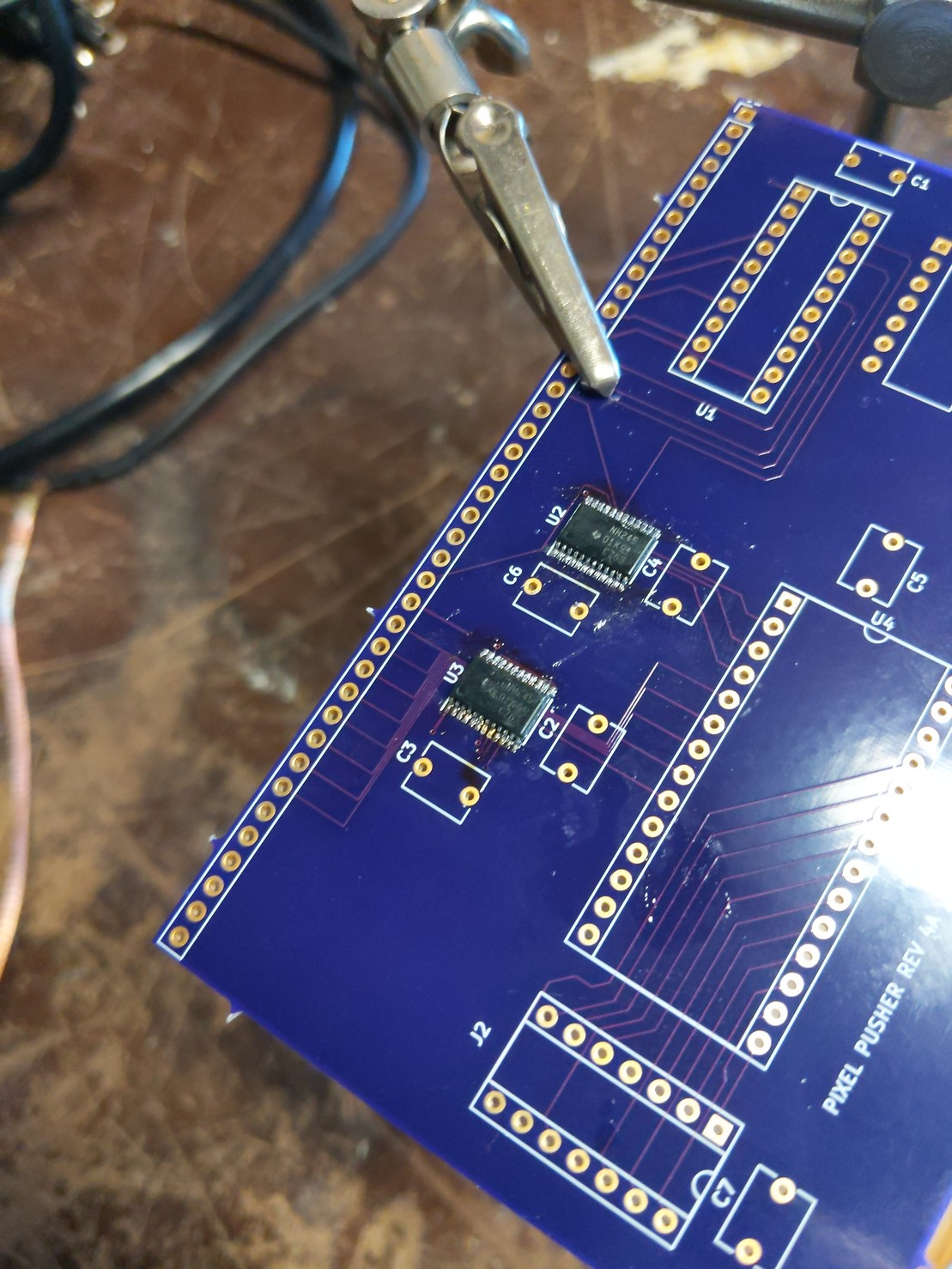 After repeating the steps above for the second level shifter chip, I'm left
with a board with two nicely soldered, surface-mount chips. Thankfully, I
didn't discover any more missing connections!
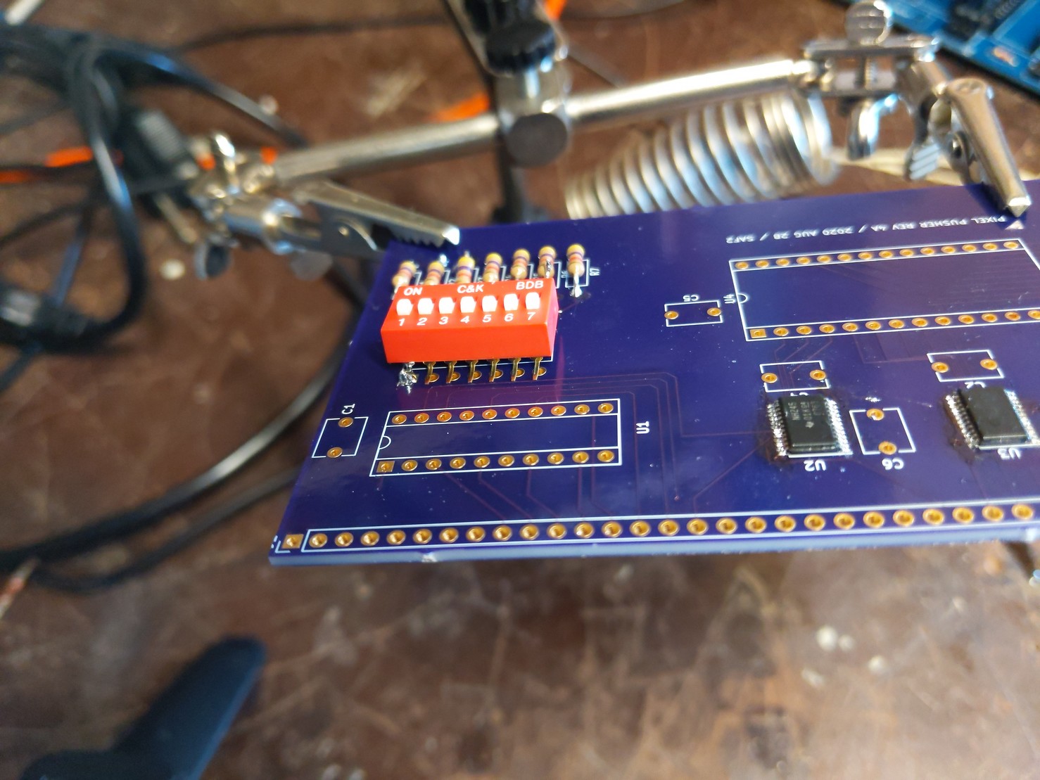 I found out the hard way that the footprint used for the DIP switches (which
should have been a normal 14-pin DIP footprint) was too wide for the actual
switch. Thankfully, I could splay the legs of the switch out and make surface
contact with all the holes on the component-side of the board. Since all the
holes are fully plated through (per OSH Park's website and as continuity checks
confirm), treating the DIP switch package as a surface mount device instead of
a through-hole device provides the extra length needed to ensure good contact
with the rest of the circuit.
So, I splayed the pins out, tacked opposite corners of the DIP switch down,
and ...
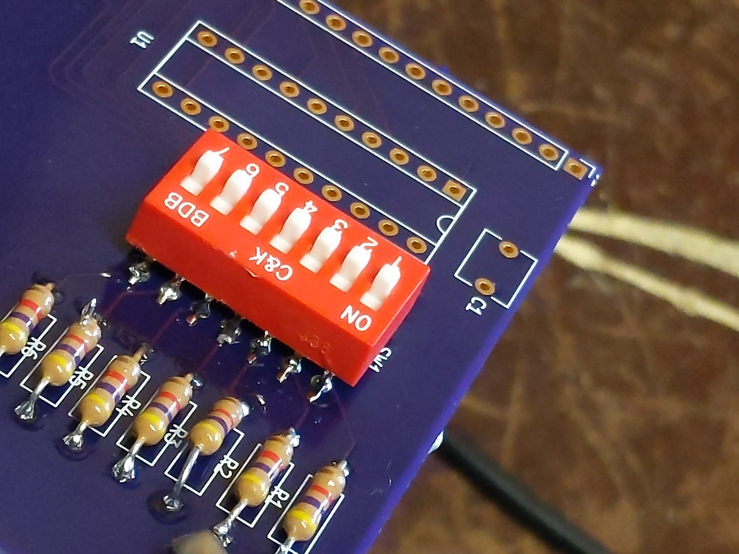 proceeded to blob solder on the remaining pins. I then set the DIP switches so
that the card will respond to I/O ports 6Eh and 6Fh (not shown). I then set
the DIP switches on the breadboard prototype to respond to I/O ports 6Ch and
6Dh, which would allow me to have both VDC-IIs in the RC2014 circuit at the
same time without contention.
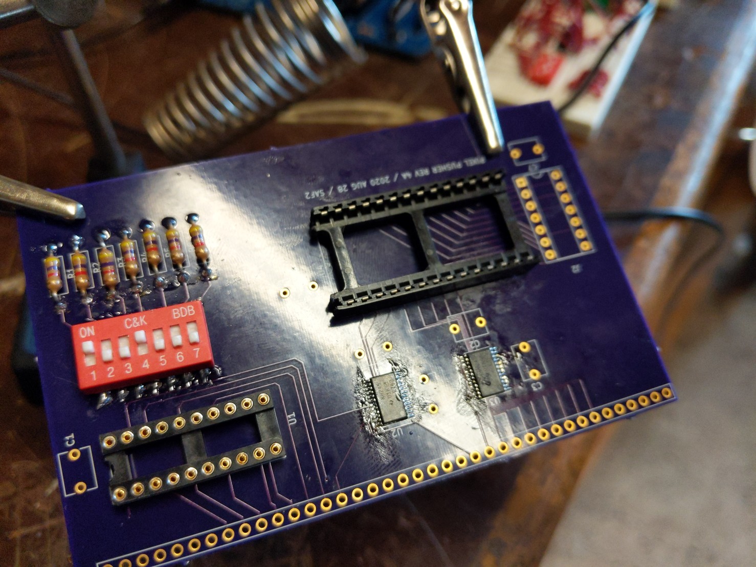 Next, I needed to fit a 28-pin, 0.6" wide socket for the TinyFPGA BX module.
However, I didn't have any on-hand. Disturbing; I believe I ordered these some
time ago via Amazon. Whatever, no biggie; I instead took a spare 40-pin socket
I had available and chopped off six pins on either side. The result fits
perfectly.
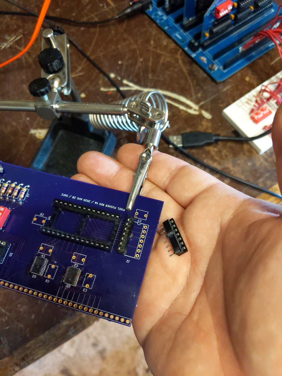 More hackery was required, as I also found out I didn't have any 14-pin DIP
sockets handy either. So, I took another 0.6" wide socket (24-pin, in this
case) and performed surgery on it to produce two make-shift 7-pin SIP sockets.
I then placed them onto the PCB, and squeezed them together until they were
0.3" apart, roughly, which you can see below.
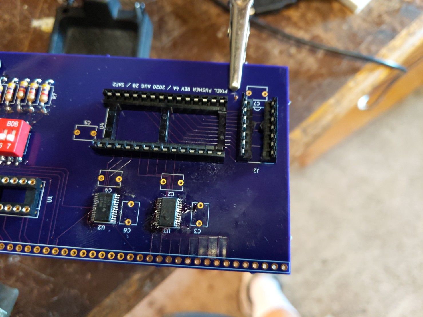 Of course, this socket is not intended to seat any chips; rather, it was
intended to be used as the receptacle for a corresponding plug on a mezzanine
board which included the analog bits of the interface. See my previous log
entry for details on its pin-out (for video output purposes at least).
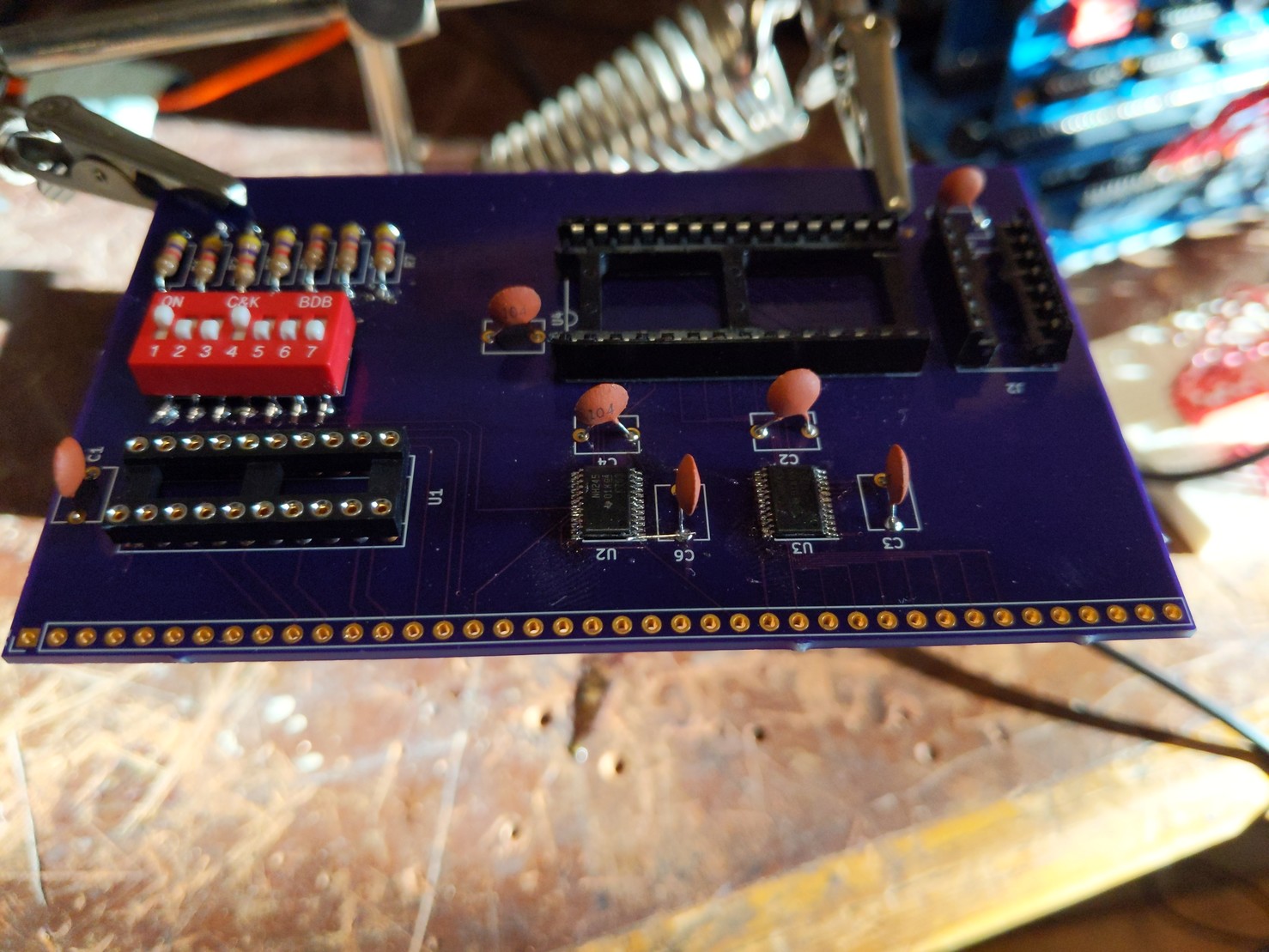 After installing the decoupling capacitors, I finally now had the means to
install the bodge required to connect U2 to 3.3V supply.
This completes the soldering of the components onto the board. After soldering
the 40-pin plug onto the board, the finished result looks really quite good, I
must say.
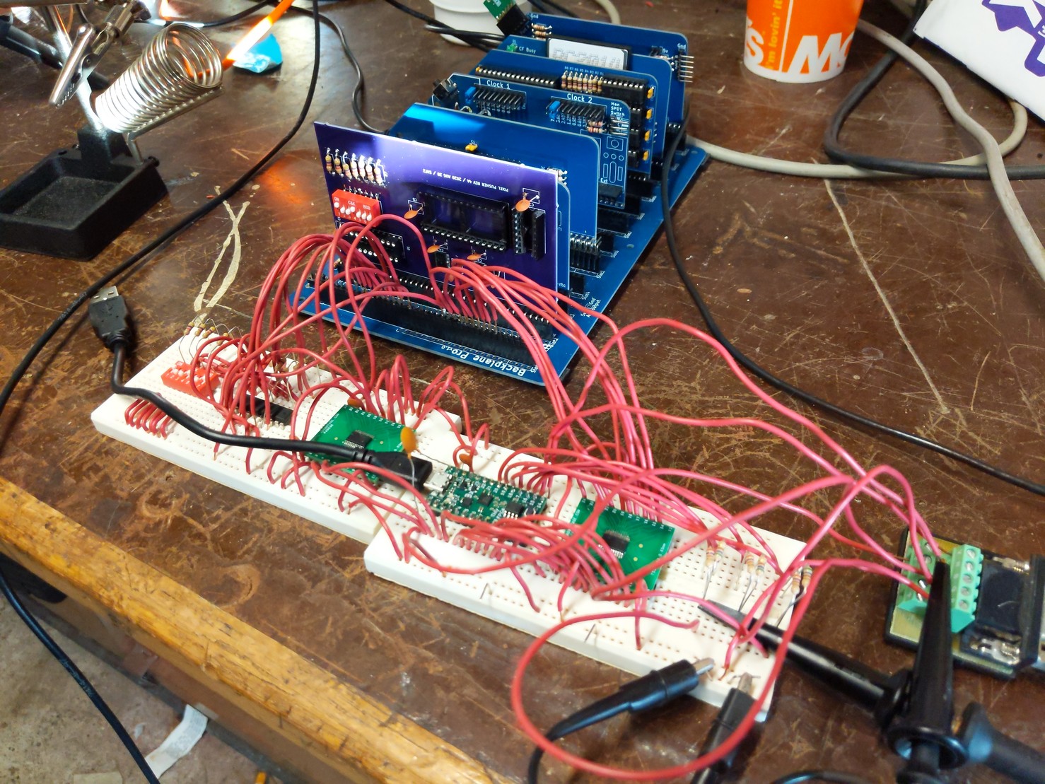 Here we see both the original breadboarded prototype of the circuit in the
foreground, and immediately behind it (the only purple PCB there), we find the
Pixel Pusher Revision 4A board sitting in the RC2014 backplane. These two
circuits are (as far as my checks can confirm) electrically identical, so once
I populate the Pixel Pusher card with a TinyFPGA BX and the 74HCT688 comparator
chip, it should "just work" (where "work" is defined as the card should match
the observed behavior, bug for bug and feature for feature, as the breadboarded
circuit).
I ran out of time to perform testing; so, I'll need to wait until later to see
how it performs.
Prototype PCBs ordered.
09/01/2020 at 23:53
That is all. ETA on delivery is September 11, but I probably won't get
around to assembling one until some time after that.
PCBs Designs Finished
08/29/2020 at 02:02
I've completed the initial design for the printed circuit boards for the RC2014
computer. This is my very first PCB design in KiCad, along with my very first
4-layer board, so I really have no idea what I'm doing. That said, I did it
anyway, and the first batch of printed circuit boards have been submitted to
OSH Park.
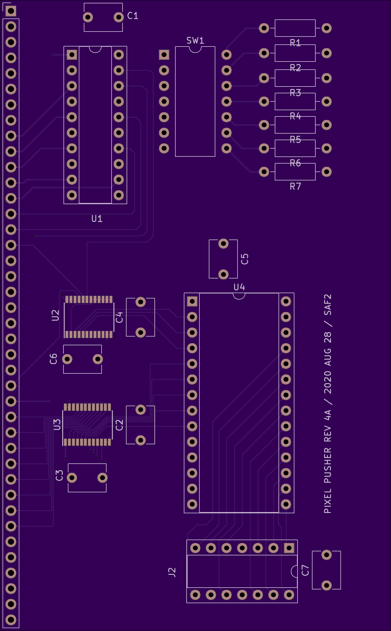 Nothing has been ordered yet, however. I'm waiting to hear back from OSH's
support team on one question I had after uploading the designs. But, assuming
everything checks out, I'll be placing an initial order for three circuit
boards.
The circuit boards will make use of a 14-pin DIP socket as a connector for a
mezzanine circuit board. This connector provides access to 11 digital I/Os on
the FPGA, which is enough to drive an analog VGA port using discrete resistor
DACs. The pin-out of the J2 connector (as it's currently labeled on the PCB)
is as follows:
| Description | Pin | Pin | Description |
|-------------+-----+-----+-------------|
| R2 | 1 | 14 | R1 |
| R0 | 2 | 13 | G2 |
| G1 | 3 | 12 | G0 |
| GND | 4 | 11 | +3.3V |
| B2 | 5 | 10 | B1 |
| B0 | 6 | 9 | n.c. |
| HSYNC# | 7 | 8 | VSYNC# |
This pin-out supports a 512 color display. However, if you reprogram the FPGA
for other tasks, it can be used to, e.g., control SPI or I2C devices, and so
forth.
One pin is no-connect, and is intended to allow future mezzanine boards to
auto-detect which version of the connector they're plugged into. For example,
if a later revision of the video card supports 32768 colors, I'll need to add 6
more pins (at least). A 32K-color mezzanine designed for the 20-pin connector
can still plug into and inter-operate with the older 14-pin connector, if it
pays attention to pin 9. (Although, how it is to pay attention to pin 9
remains to be specified. YAGNI.)
Strip Buffers Done, VDC-II Core Usable (more or less)
05/30/2020 at 22:09
I've completed the strip buffer implementation, the block memory arbiter, and
the video fetch engine, and mated it with the MPE. This provides the host
processor the ability to manipulate the display memory and we can finally
observe the effects on the screen!
After setting the video mode to 80x30 text display, placing the text display at
address 0000H and the attributes at 0C00H, you can run this little program in
BASIC on the RC2014 to look at the first half of the VDC's character set
(glyphs 0 through 255).
1000 OUT 110,18:OUT 111,0
1010 OUT 110,19:OUT 111,0
1020 OUT 110,31:FOR I=0 TO 2399:OUT 111,(I AND 255):NEXT I
1030 OUT 110,18:OUT 111,12
1040 OUT 110,19:OUT 111,0
1050 OUT 110,31:FOR I=0 TO 2399:OUT 111,(I AND 15):NEXT I
BASIC is slow enough that you don't need to worry about waiting for the MPE to
finish stores into video memory; if you write this code in machine language,
however, you'll need to remember to wait on the VDC. In any event, it should
produce something resembling the following (if attributes are turned on).
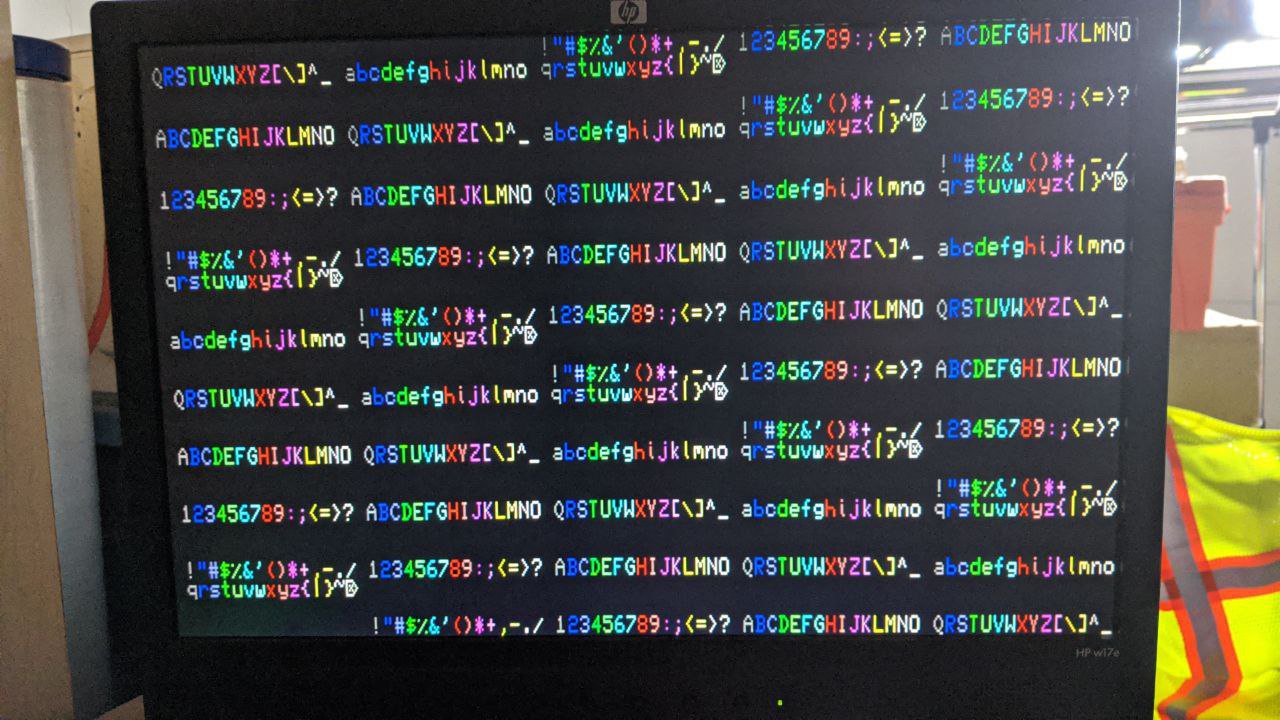 If you turn off the attributes and set the foreground and background colors to
bright green and dark grey, you'll get a display which kinda sorta looks like a
Commodore PET (or the Commodore 128 when it boots in 40-column mode).
Bitmapped graphics mode works as well. If you ran the previous code above,
then try executing the following listing, you should see high resolution
"garbage" on the screen, complete with color attributes applied. NOTE:
the TinyFPGA BX is only big enough to contain 16KB of video RAM, as that's all
the block RAM it has available. Thus, the 640x480 VGA display is going to have
several repeated slices showing the same data. That's normal and expected.
OUT 110,25:OUT 111,INP(111) OR 128
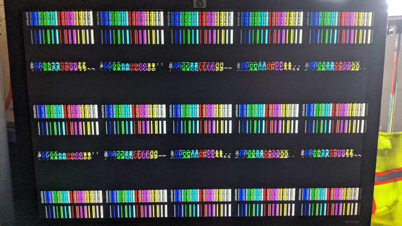 Since the TinyFPGA BX only supports 16KB of RAM, there's no way to fit
attributes in with a full-screen bitmap image. So, you'd typically turn off
attributes to have a proper monochrome display. However, the VDC-II doesn't
yet support scan-doubling, so it renders the screen at full resolution whether
you like it or not.
OUT 110,25:OUT 111,INP(111) AND &HBF
OUT 110,26:OUT 111,&H51
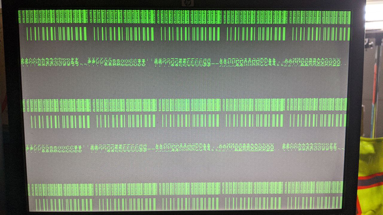 Interesting how you can see where the screen data resides, where the attribute
data resides, and where the character set resides in VDC memory. :)
So, now that I've demonstrated that I have a workable, usable display, I
figured it was time to try and write something that is "useful", in the sense
that it is representative of a typical program most would consider to be
useful. I decided to work on a simple clock application, and you can find
the latest source code to it in the repository.
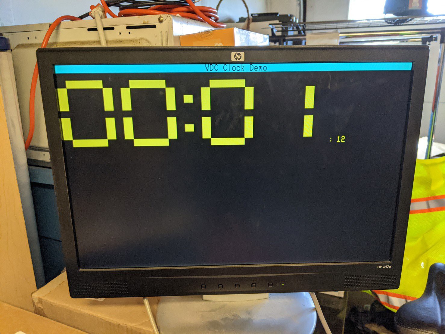
Here's what it looks like when it first starts up.
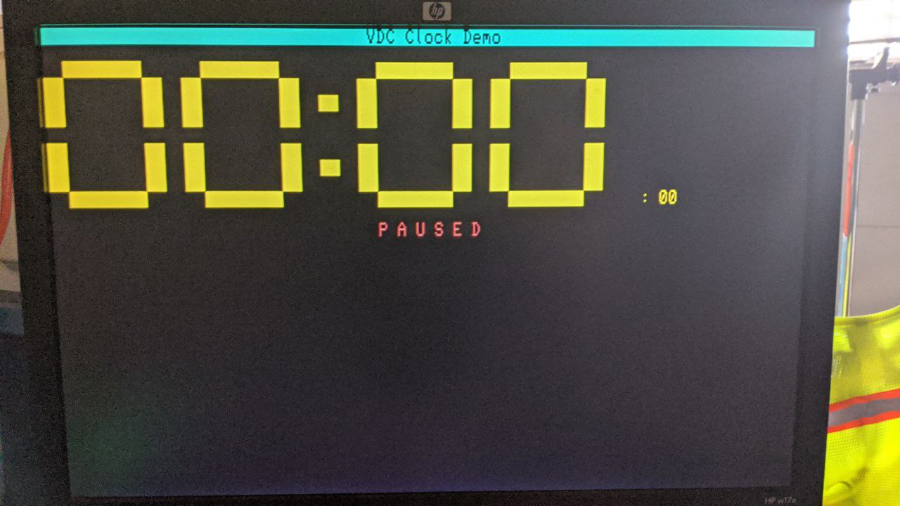 To unpause the clock, you tap the P key on the RC2014 terminal. It will then
start counting up, in roughly 1 second intervals. Kinda sorta like this:
VIDEO: RC2014 running VDC-II core on FPGA, Clock Demo
While working with the code, I ran into two hardware bugs. One of which I knew
about from earlier development; however, a new bug has manifested. The bugs
are:
1. If polling the status register too fast, it will corrupt subsequent MPE
operations. I've additionally discovered that this will even manifest when not
using block-copy or block-write mode. It can also show up as corrupted VDC
registers as well; it's not restricted to affecting video memory.
2. And the latest bug I discovered was that, for some reason, reading the data
register does not automatically update the update pointer. Thankfully, writes
to this register does not cause issues.
What's Next?
In no particular order:
1. Well, I'd like to finish the development of the clock; there are a few added
niceties I'd like to throw in.
2. I need to finish designing the printed circuit board for the VDC-II RC2014
card.
3. Implement missing features, like hardware cursor, row address increment
support, underline attribute support, etc.
4. Fix known hardware bugs.
Still a ways to go before I can declare this project "done"; however, it's now
certified to be in a usable state, which is quite exciting!
More Thoughts on Video Refresh
05/12/2020 at 16:22
The VDC video modes all assume that the VDC can access arbitrary video RAM with
impunity. While you can fetch character and attribute data sequentially,
resolving character codes to font data requires a potentially fresh hit to
video memory, starting at either BASE+(16*code) or BASE+(32*code), depending on
the configured character height.
Even if the character codes increase monotonically, the memory fetched will
have 16- to 32-byte gaps in between referenced bytes. This breaks the optimal
access pattern for synchronous memories, all of which are optimized for
sequential access patterns. A good rule of thumb for synchronous memories is
that every time you need to skip around in memory will cost you 10 cycles of
latency.
Although it is possible to sequentially fetch character and attribute data,
they occupy different segments of video memory, necessitating two video base
pointers and two processing engines. Correspondingly, if you fetch 8 bytes of
character data, you must also fetch 8 bytes of attribute data. The two bursts
of data must be synchronized with each other externally to the memory fetch
units.
Character and attribute bursts can happen in any order (e.g., attributes can be
fetched ahead of character codes), but they must always be adjacent. Moreover,
both character and attribute bursts must occur prior to font resolution, as
attributes provide the 9th character code bit.
On the iCE40LP8K I'm currently targeting, a ping-pong line buffer, such as what
I used to implement the MGIA on the Kestrel-2 and -2DX, will be prohibitively
expensive. The space for a single line buffer of 256 characters would require
2048 DFFs (and, thus, logic elements). We would need two of these, so that the
memory fetch logic can fill one buffer while the other is used for video
refresh. Note that the FPGA only has 7680 logic elements.
Because they switch roles only on HSYNC boundaries, full-line buffers must be
large enough to accommodate the widest display supported. The VDC-II register
space supports 256 characters (all 8 bits of R1 are significant). If we
couldn't accommodate a pair of line buffers large enough to support 256
characters, then we would need to ignore upper bits of register R1, which would
break 8563 VDC compatibility.
Video data (resolved character/bitmap data plus corresponding attribute
information) must be available when horizontal display enable asserts, since
that's when we must start shifting out video data.
All of these problems interact. Thankfully, besides the queue-based approach I
discussed in a previous log, there's another approach to work around these
matters.
Another Solution
Instead of using full-line buffers, we use a pair of ping-pong "strip" buffers.
Each strip is 4, 8, or 16 characters, depending mainly on externally imposed
video memory latency requirements. For the purposes of this description, let's
assume a 4-character strip.
A strip buffer contains two bytes for each character column it supports: an
attribute byte and a bitmap byte. When attribute data is fetched, only the
attribute bytes are updated. When character data is fetched, only the bitmap
bytes are updated. The interface presented to the dot-shifter logic, however,
always presents a 16-bit attribute/bitmap value pair.
To minimize the time needed to provide the complete set of data for a strip,
attribute data should be fetched first. That way, when character data is
fetched, we can stream data not only from video memory but also (in parallel)
the strip buffer to provide the complete 9-bit character code to the font fetch
unit. The font fetch unit can then resolve the character code to a bitmap
byte. For this to work, font data must reside in fast FPGA block RAM.
The following table illustrates the memory fetch access patterns with
0-wait-state memory on a pipelined Wishbone B4 interconnect to video RAM and an
asynchronous strip buffer read port. You could typically find this access
pattern when placing character, attribute, and font data in block RAM.
Assuming we reference video memory at the same speed as the dot-clock, we can
reload the strip with video data in just 13 pixels. Note that a four character
strip with 8 pixels per character contains 32 pixels, giving us ample time to
refill the strip buffer. Four characters at 3 px/char would have only 12
pixels, so we would expect to see visual artifacts under those conditions.
You'd want at least 4 px/char in order to ensure a clean display.
| Cycle | VRAM Address | VRAM Data | SBUF Read Address | SBUF Write Address |
|:------|:-------------|:----------|:------------------|:-------------------|
| 1 | ATTRPTR+0 | | | |
| 2 | ATTRPTR+1 | a0 | | ATTR0 |
| 3 | ATTRPTR+2 | a1 | | ATTR1 |
| 4 | ATTRPTR+3 | a2 | | ATTR2 |
| 5 | CHARPTR+0 | a3 | | ATTR3 |
| 6 | CHARPTR+1 | ch0 | | CHAR0 |
| 7 | CHARPTR+2 | ch1 | | CHAR1 |
| 8 | CHARPTR+3 | ch2 | | CHAR2 |
| 9 | FONT(ch0) | ch3 | PAIR0 | CHAR3 |
| 10 | FONT(ch1) | bm0 | PAIR1 | CHAR0 |
| 11 | FONT(ch2) | bm1 | PAIR2 | CHAR1 |
| 12 | FONT(ch3) | bm2 | PAIR3 | CHAR2 |
| 13 | | bm3 | | CHAR3 |
Below illustrates the same refresh attempt, assuming that both attribute and
character matrix data is located in a HyperRAM chip, while font data continues
to be confined to block RAM. In this case, we see it takes 23 pixels to reload
the strip buffer with video data, thanks to the HyperRAM access latency. As
you might imagine, four characters of 4 pixels each will not be sufficient to
refresh the display without artifacts. Therefore, if you intend on using a
character-mode display with narrow characters, you should strive to keep the
matrices inside VDC-II block memory space. Where possible, use external memory
resources only for bitmapped video modes, or, make sure to use sufficiently
wide characters.
| Cycle | VRAM Address | VRAM Data | SBUF Read Address | SBUF Write Address |
|:------|:-------------|:----------|:------------------|:-------------------|
| 1 | ATTRPTR+0 | | | |
| 2 | (wait) | | | |
| 3 | (wait) | | | |
| 4 | (wait) | | | |
| 5 | (wait) | | | |
| 6 | (wait) | | | |
| 7 | ATTRPTR+1 | a0 | | ATTR0 |
| 8 | ATTRPTR+2 | a1 | | ATTR1 |
| 9 | ATTRPTR+3 | a2 | | ATTR2 |
| 10 | CHARPTR+0 | a3 | | ATTR3 |
| 11 | (wait) | | | |
| 12 | (wait) | | | |
| 13 | (wait) | | | |
| 14 | (wait) | | | |
| 15 | (wait) | | | |
| 16 | CHARPTR+1 | ch0 | | CHAR0 |
| 17 | CHARPTR+2 | ch1 | | CHAR1 |
| 18 | CHARPTR+3 | ch2 | | CHAR2 |
| 19 | FONT(ch0) | ch3 | PAIR0 | CHAR3 |
| 20 | FONT(ch1) | bm0 | PAIR1 | CHAR0 |
| 21 | FONT(ch2) | bm1 | PAIR2 | CHAR1 |
| 22 | FONT(ch3) | bm2 | PAIR3 | CHAR2 |
| 23 | | bm3 | | CHAR3 |
As long as the strip is wide enough to support the longest latency of the video
memory, then we simply switch strip buffers after rendering the last pixel of a
strip. Switching strip buffers should also commence fetching the next strip's
worth of video data as well.
This algorithm should work to keep the video data sequenced for video refresh
while it is in the middle of the scanline. The next issue to tackle is how to
sequence the *first* strip, along the left-most edge of the display. The CRTC
doesn't have enough information to trigger the first strip fetch exactly 4-16
characters ahead of the left edge of the display. The only events we can rely
upon for this is:
1. The negation of the display enable signal.
2. The assertion of HSYNC.
3. The negation of HSYNC.
I believe each of these events would serve a unique role. We would accumulate
the address increment value to the fetch pointers when display enable falls.
We would schedule the first strip fetch at the assertion of HSYNC.
Bitmap mode can be implemented by simply not resolving character codes into
font bitmaps. "Monochrome mode" (that is, where one turns off attributes) can
be implemented by having the attribute fetch logic just synthesize default
attribute values based on register settings.
Thoughts on Handling Video Refresh
05/09/2020 at 01:14
At first, I thought the best approach to handling video refresh with the VDC-II
core was to use ping-pong scanline buffers, like how the Kestrel-2's MGIA core
did its video refresh.
I think that's still an approach that could work; but, I have to wonder if it
wouldn't be simpler to just use a collection of modestly-sized queues instead?
At its core, a video controller consists of two parts: the timing chain (which
I've already completed) and what amounts to a glorified serial shift register.
By its very nature, getting data from video memory to the screen happens in a
very pipelined fashion. Everything is synchronized against the dot clock, and
usually, also a character clock. Competing accesses to video memory, however,
could cause a small amount of jitter; perhaps enough to cause visible artifacts
on the display. Queues would apply naturally here, and can smooth out some of
that jitter.
The disadvantage to using queues, though, is that video RAM access timing is
much more stringent than with whole-line ping-pong buffers. I can't just slurp
in 80 bytes of character data, 80 bytes of attribute data, and then resolve the
characters into bitmap information (totalling 240 memory fetches), then sit
around until the next HSYNC. I will need to constantly keep an eye on the
video queues and, if they get too low, commence a fetch of the next burst of
data.
The disadvantage to using ping-pong buffers, though, is a ton of DFFs and logic
elements will go into making up the buffers. Like, if I want to support a
maximum of 128 characters on a scanline (128 characters at 5 pixels/character
can also provide a nice 640-pixel wide display), I'll need 384 bytes worth of
buffer space: 128 for the character data, 128 for attribute data, and another
128 for the font data for each character on that particular raster. 384*8=3072
DFFs, and if memory serves, I think you need one LE per DFF. There are only
7680 LEs on the FPGA. I can't use block RAM resources because those are
already dedicated for use as video memory (in this incarnation of the project,
at least; I'll work on supporting external video memory in a future design
revision).
So, while it's possible to implement a design using ping-pong buffers, it would
make very inefficient use of the FPGA's resources. Since logic would be strewn
all about the die, it could also introduce sufficient delays that the circuit
fails to meet timing closure.
The more I look at things, the more I think using a set of fetch queues makes
sense. I'm thinking a design similar to this would work:
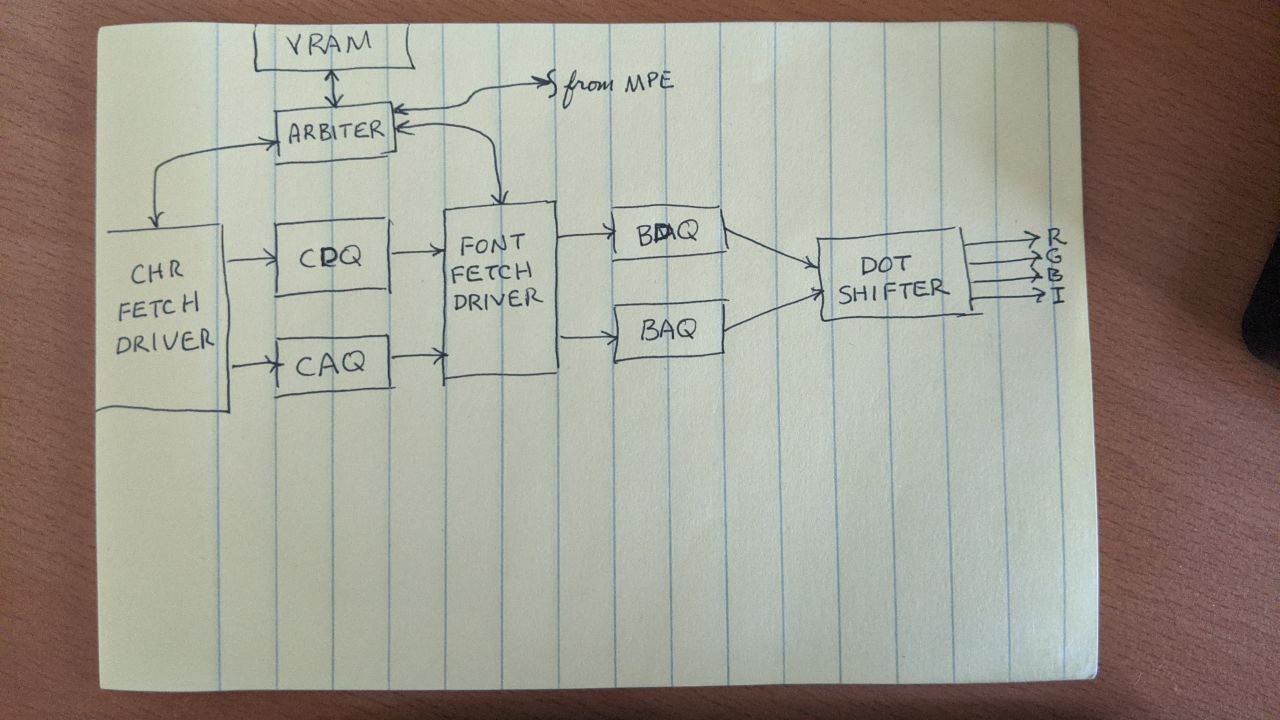 Key:
* CDQ -- Character Data Queue
* CAQ -- Character Attribute Queue
* BDQ -- Bitmapped Data Queue
* BAQ -- Bitmapped Attribute Queue
Of course, I'm still not quite sure how to handle bitmapped graphics mode. The
most obvious approach (which isn't always the best approach!) is to configure
the font fetch driver to just pass through the data. But, this will require
some additional though.
16KiB Video RAM, CPU Data Port Finished
05/08/2020 at 05:52
I'm happy to report some progress made on the VDC-II project. I finished the
CPU-to-video RAM interface. This includes block write and block copy functions
from the original Commodore 8563 VDC chip. Only one small problem...
If you try to use the VDC-II chip as documented by Commodore, where you poke a
register address, then wait for the chip to be ready, then poke a data value
into a register, the DMA engine (what I call the Memory Port Engine, or MPE)
corrupts video memory during a block operation.
However, if you poke the address, then poke the data, then wait on the ready
flag, everything works perfectly! This breaks backward compatibility with
Commodore's VDC, which makes me sad. It should work both ways; but, at least I
have a viable software work-around.
Next steps are to implement the video fetch logic and the memory bus arbiter
that will keep the different modules from stepping on each other's toes. If I
can fix the aforementioned bug, that'd be great; but it's not a priority for
me.
Can a VDC-II Support a 8K Display?
04/27/2020 at 01:54
I got an interesting (if not to be taken seriously) question on my Mastodon
feed today: 8K VDC-II when?
For now, let's focus exclusively on the CRTC capabilities, and completely
ignore the logistics of getting pixels onto the screen. The latter
implementation details will necessarily have to change regardless, so I take it
as a given that the VDC-II as I'm currently envisioning it cannot support
anything greater than a 1K display.
So, let's look at what the current VDC-II's CRTC registers can do, in regards
to 8K, 4K, 2K, and 1K displays, respectively. (By comparison, a 640x480 VGA
display is 0.8K.)
The Original Question: 8K VDC-II When?
I'm pretty sure the CRTC interface of the VDC-II will need to be changed to
support an 8K display. An 8K display resolution seems to be 7680x4320, at
least that's what Wikipedia tells me. The VDC-II CRTC supports a maximum
character cell width of 16 pixels; 7680/16=480, which is too wide for the 8-bit
horizontal displayed register to hold on its own. Thus, the VDC will need
either adjunct registers or an all-new 16-bit interface to cope with the
additional bits needed for horizontal timing.
So, at present, the VDC-II is not able to handle 8K displays. Sorry. It
probably can be made to support these large resolutions with relative ease;
but, it'll require more investment in the hardware description, an FPGA fast
enough to cope with the insane dot clock speeds, and testing with compatible
display hardware.
What about 4K Displays?
It's so close! While the vertical resolution is achievable with relative ease,
the horizontal direction proves to fall just short of the minimum required
functionality.
A typical resolution for a 4K display with consumer hardware is 3840x2160, so
I'll use that for my calculations. 3840 can be divided into 256 characters at
15 pixels each. The VDC-II, as I've currently defined it, does not support 256
characters; it only supports 255. However, a revision can be made to the
hardware description where plugging a 0 into the horizontal displayed register
(R1) could be interpreted as meaning 256 characters. It would require
redesigning the display-enable circuit to be a bit more clever than "assert
display enable as long as the display counter is non-zero."
The bigger problem is the horizontal total register (R0), which is used for
HSYNC timing pulse generation. This requires more than 256 characters; if you
think about it, the 256 characters discussed above are those which are the
visible part of the display. So, unfortunately on this basis alone, the VDC-II
cannot support a 4K display.
Things are a bit better in the vertical dimension, however. At 2160 pixels, we
can reasonably fit 216 10-pixel tall characters on the screen, 135 16-pixel
tall characters, or 108 20-pixel tall characters. All of these configurations
are well within the realm of possibility for the current VDC-II design.
What about 2K, then?
2K video is a different matter. According to Wikipedia, the largest recognized
2K resolution is 2048x1080. From the point of view of the VDC-II's current
CRTC implementation, this resolution is a cake walk.
With 16-pixel wide characters, the horizontal displayed register would be set
to 128, which (if you follow the rule of thumb that active video takes 75% of
the horizontal display time) means the horizontal total register would probably
be somewhere in the vicinity of 170. These are all easily within the range of
the 8-bit character counters as currently found on the VDC-II.
Similarly, in the vertical dimension, we're looking at a vertical displayed
setting of 135 (for an 8px tall font), 90 (for a 12px tall font), or 67 (for a
16px tall font). Note that the CRTC supports up to 32px tall fonts.
What Else is Needed?
One problem with 2K displays and higher is the need for 16-pixel wide fonts.
Commodore's VDC only supported 8-pixel wide font data. I wasn't planning on
supporting double-width fonts until I had a real need for them, but it is (as
can be seen above) a pretty obvious extension that can be made to a future
revision of the VDC-II core.
Obviously, with increased resolution comes the need for increased numbers of
bits to hold the required numbers. Horizontal total and displayed registers
are 8-bits wide presently. To support 8K, they'll need widening to 10- and
9-bits, respectively. It's possible similar expansion will be needed for the
vertical direction as well.
It's unknown how wide the sync widths (in either axis) are for these video
modes, so it's conceivable we'll need to add more bits to hold that information
as well.
Finally, you'll need enough video memory to support your preferred display
mode. Assuming a 16x16 pixel font for an 8K display, character mode screens
will take up 259.2 kilobytes just to hold the character and attribute data!
Contrast that with the VDC's original memory compliment of 16KiB (64KiB
possible). Moreover, the font data alone will need to be 16KiB in size for 8-
to 16-pixel tall fonts, and 32KiB for anything bigger.
Conclusion
Is it technically feasible that a VDC-II can be synthesized to support an 2K,
4K, or 8K display? Yes! These are not insoluble problems, and perhaps
surprisingly, very little resources are required to pull it off. The biggest
concern will be in how the VDC-II fetches from memory, how the advanced
features are exposed in the CPU-visible register set, and in supporting the
breakneck speeds required for these high resolutions.
But, will I be the one to produce a VDC-II that can support an 8K movie theater
display? Almost certainly not. Sorry!
CRTC Finished; First Pixels Displayed
04/26/2020 at 16:41
Treating the VDC as a superset of the 6545 CRTC chip has finally allowed me to
complete both the horizontal and the vertical sync generators. Additionally,
both generators use the same subcircuit description. You can see how I
configure two instances of the SyncGen class to work together in the VDC module
file.
After getting the sync generators working and bug-fixed, I was able to hook the
RGBI outputs to various internal signals to see what is happening. It was at
this time that I wired up my first resistive DAC as well.
First, I hooked the RGBI outputs up to the vertical sync generator's character
counter, to display horizontal color bars. At first, the colors were
distorted; I thought that my resistor values were off (I just grabbed the
closest values I could find to the ideal resistors). But, after fixing the
hardware description to account for the display-enable signal, the colors fixed
up nicely. Lesson learned: even though an LCD doesn't sling electrons at a
phosphor like a CRT, you still need to blank the outputs so that the monitor
has a proper black reference level.
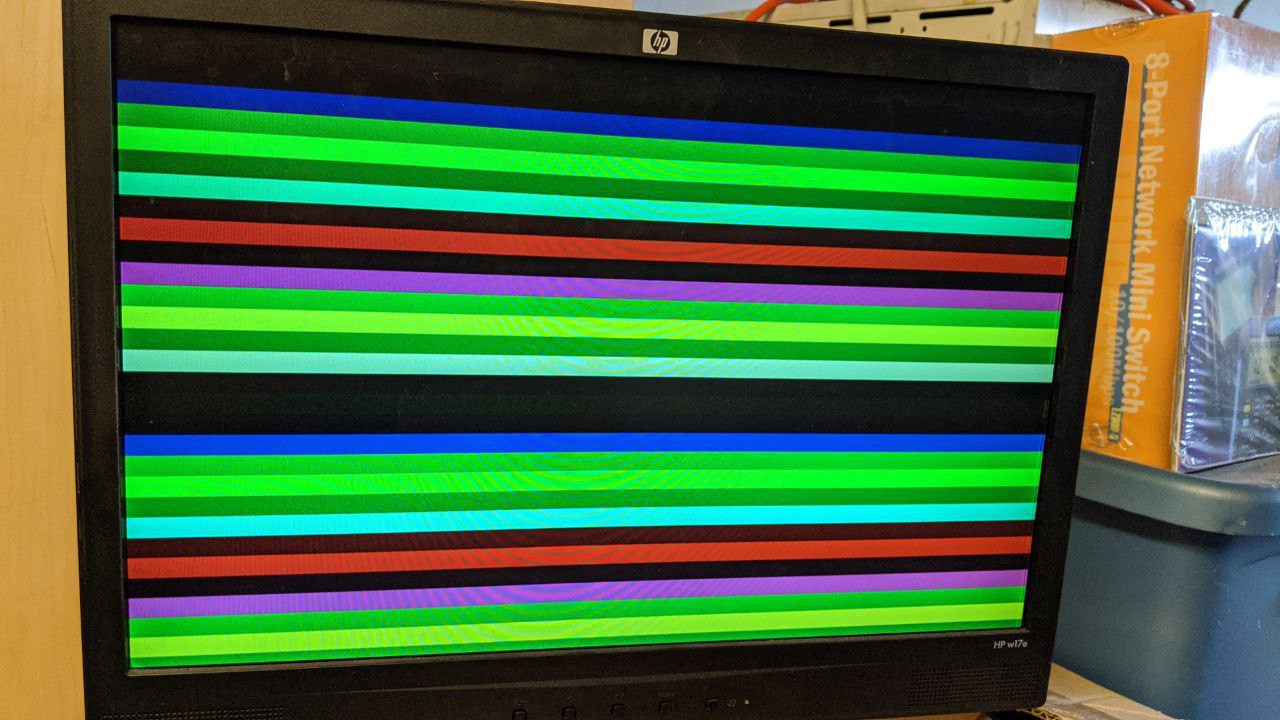 (without blanking the video)
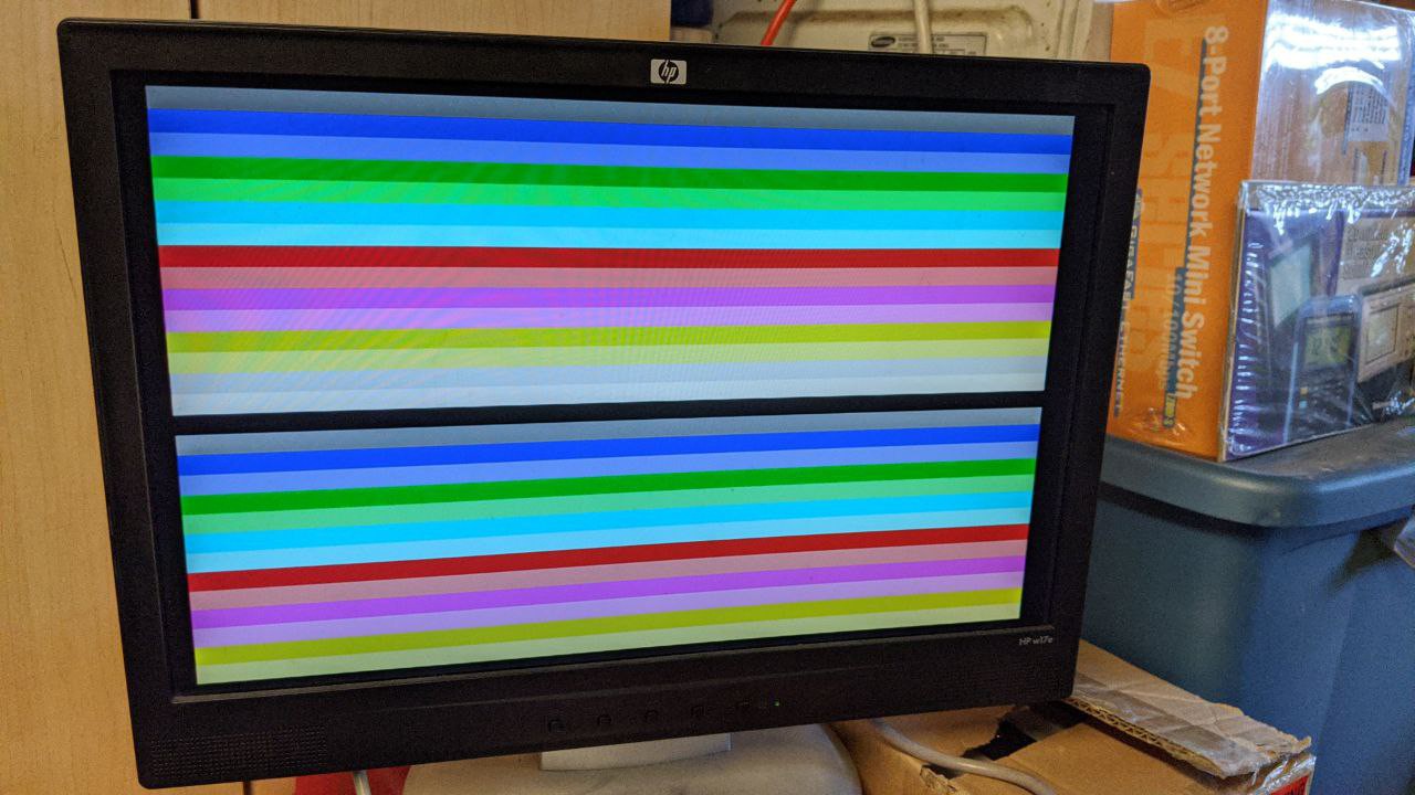 (with blanking the video)
For funsies, I then rewired the RGBI outputs to show the horizontal character
counter next.
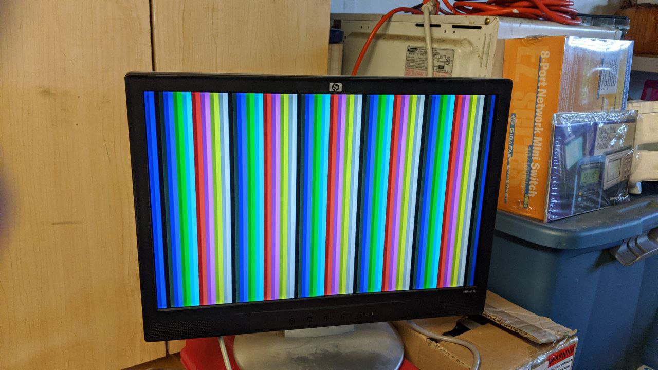 Finally, I decided to show the "character matrix" of the VDC output by tieing
the red signal to the HSYNC generator's xclken output, and green to VSYNC's
xclken output. The playfield will be illustrated by driving the intensity
output. This results in a nice graph paper-like effect and it visually shows
how several of the VDC registers interact. It's really neat to play with!
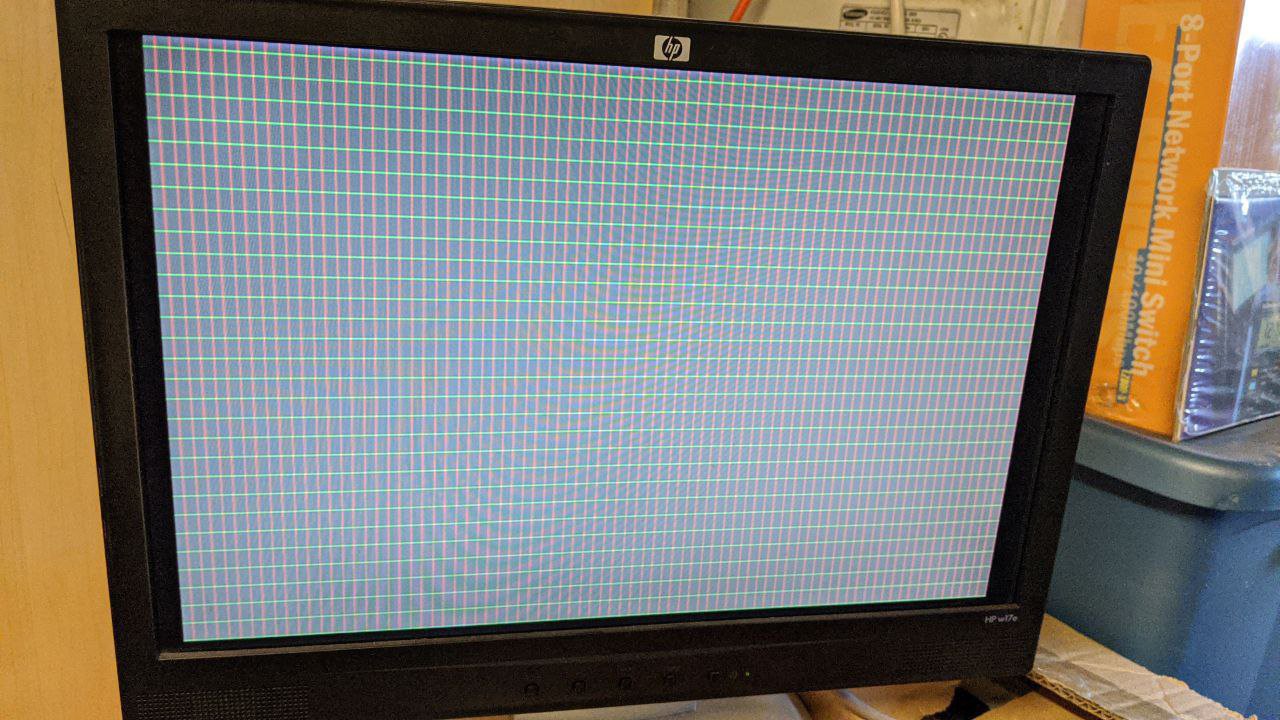 (80x30, using 16-pixel tall characters)
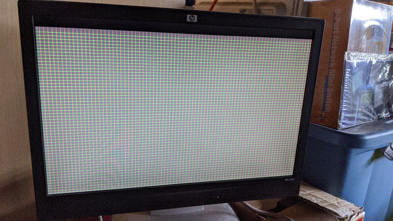 (80x60, using 8-pixel tall characters)
Sharp-eyed viewers might notice one final bug that needs squashing: notice the
top row of characters is elongated? That's because the vertical total adjust
circuitry does not negate the display-enable signal while operating. This is a
very simple fix to implement.
BASIC Program to Initialize the CRTC
This program initializes the VDC's CRTC registers to produce an 80x30 character
matrix display.
10 DATA 10
200 DATA 0,99
201 DATA 1,80
202 DATA 2,82
203 DATA 3,&h2C
204 DATA 4,31
205 DATA 5,13
206 DATA 6,30
207 DATA 7,31
209 DATA 9,15
222 DATA 22,&h78
1000 READ N
1100 FOR I=1 TO N
1200 PRINT I
1300 READ R,V
1400 OUT &H6E,R
1500 OUT &H6F,V
1600 NEXT I
To produce an 80x60 display, change these lines:
204 DATA 4,64
205 DATA 5,5
206 DATA 6,60
207 DATA 7,61
209 DATA 9,7
So, what of things like horizontal and vertical smooth scrolling?
Sorry to say; but, these features will need to be considered at a later time.
Evidence now shows that Commodore engineers implemented these features outside
the CRTC logic, so I'll have to also figure out how to do the same.
What's Next?
Right now, I think my next step is to implement the 16KB of memory needed to
hold a character matrix or bitmap display, so that I can use that to start
slinging pixels onto the display. This means I'll need to implement the
infamous "busy" flag, along with registers R18, R19, and R31.
VDC Vertical Sync: One More Chance
04/24/2020 at 14:45
I stumbled recently upon the data sheet for a MOS 6545 CRT controller and
MC6845 CRT controller chips. I noticed that the vast majority of the
sync-related registers map identically to those found in the 8563 VDC, which
leads me to believe that the 8563 has a 6545 buried within it. So, if I start
out building a 6545 clone first, I should be able to build the VDC in terms of
the 6545.
Most importantly, the datasheet provides the timing diagrams I needed to
understand how the vertical total adjust and such works, as well as how the
internal counters work. H and V character counters are up-counters as far as I
can tell, while "display" counters seem to be down-counters. All these extra
counters I was needing appear to be functionality that is VDC-specific, and not
CRTC-related at all. This is good to know, because I can factor functionality
into more manageable pieces.
So, before I replace the VDC's CRT controls with those from the CGIA, I'll give
the VDC one more chance, now that I know the foundation on which the VDC is
built and have a datasheet for the 6545.
(I still think it's overly complicated, and I still think the CGIA's approach
is simpler. However, I'd prefer to maintain as much compatibility as I can.)
Breaking Compatibility: HSYNC and VSYNC on VDC is Intractible
04/23/2020 at 21:37
I'm seriously thinking about just throwing away the existing HSYNC circuitry, and switching from a character-column-based system to a pixel-addressed counter arrangement.
There are several events that need to happen along any given axis of a display:
| Event | VDC Register (Horizontal) | VDC Register (Vertical) |
|:-----------------|:----------------------------------|:----------------------------------------|
| Blanking Starts | R35 (Display Enable End) | No equivalent |
| | R22H (Horizontal Character Total) | |
| | | |
| Sync Starts | R0 (Horizontal Total) | R4 (Vertical Total) |
| | R22H (Horizontal Character Total) | R8 (Interlace Control) |
| | | R9 (Vertical Character Total) |
| | | |
| Sync Ends | R3L (HSYNC Width) | R3H (VSYNC Width) |
| | R22H (Horizontal Character Total) | R5?? (Vertical Total Adjust) |
| | | R8 (Interlace Control) |
| | | NOTE: R9 ignored here! |
| | | |
| Blanking Ends | R34 (Display Enable Start) | No equivalent? Or, R5? (I can't tell) |
| | R22H (Horizontal Character Total) | |
| | | |
| Playfield Starts | R2 (Horizontal Sync Position) | R7 (Vertical Sync Position) |
| | R22H (Horizontal Character Total) | R8 (Interlace Control) |
| | | R9 (Vertical Character Total) |
| | | |
| Playfield Ends | R1 (Horizontal Display Total) | R6 (Vertical Displayed) |
| | R22H (Horizontal Character Total) | R8 (Interlace Control) |
With the 8563/8568 VDCs, these events are encoded in a variety of registers
which, frankly, make no sense and makes for hardware which is significantly
more complicated than it needs to be. It has taken me several weeks worth of
study and a corresponding amount of experimentation with emulators to finally
understand how to implement a compatible HSYNC generator, and to figure out how
horizontal scrolling would work.
I've been trying to figure out a corresponding theory of operation for the
VSYNC generator, but to no avail. It seems to defy any rational explanation.
Despite the registers seeming to indicate they are common circuits under the
hood, it turns out that there's enough minute edge- and special-cases that
differ between HSYNC and VSYNC generation that they each would require their
own formal specification.
I'm not sure I want to go down this rabbit hole.
It is especially weird that the VDC has separate registers for controlling
blanking along the X-axis, but not on the Y-axis.
Contrast this with my CGIA concept, which I'd intended for use with the
Kestrel-3 project. It uses pixel/line up-counters and magnitude comparators to
trigger events. Horizontal control circuitry always works in units of pixels.
Vertical control circuitry always works in units of raster lines. Both have a
similar set of registers. No exceptions, and thus, no strange surprises.
Plus, this approach directly supports features like raster interrupts, which
are notably absent on the original VDC.
The other criticism I have of the VDC approach is its extreme reliance upon
down-counters for almost everything, key word being "almost." In both X- and
Y-axes, there are separate down-counters for specific purposes (e.g., to
control the horizontal display enable, for example), but up-counters for other
purposes (e.g., vertical smooth scroll depends upon a down-counter, but knowing
which raster line to fetch for character font data depends on a corresponding
up-counter that holds the same information.) This is incredibly wasteful of
resources, to say nothing of how confusing it is to keep the design in your
head.
In conclusion, although I'm satisfied that I've been able to figure out HSYNC
behavior, I'm simply not able to crack the VSYNC behavior nut. I've spent
weeks on this problem, but haven't gotten any further than defining how the
display is generated without support for vertical smooth scrolling or the
vertical total adjust. Without a coherent method of generating HSYNC and
VSYNC, we can't get a stable display. For this reason, I'm deeply inclined to
change the programming interface for the VDC-II away from VDC-style CRT control
and replacing it wholesale with CGIA-style CRT control instead.
I really, really wanted to maintain backward compatibility with the VDC on this
particular aspect. But, I see that is proving to be more expensive in terms of
my time than I had hoped. Perhaps some external contributor can provide a
compatible hardware definition in the future. For now, I think going with the
CGIA CRT controls is the right choice for me.
Thoughts on Supporting Horizontal Smooth Scrolling
04/19/2020 at 21:41
Ever wondered why the C128's VDC has such a strange way of supporting smooth
scrolling? I did, and I'm sure I'm still wrong, but I think I've gotten pretty
close to the truth. Especially as my goal with VDC-II is to maintain backward
compatibility where it makes sense.
What follows is a brain-dump, me rubber-ducking with myself, on this very
topic. Enjoy! While working on the VDC-II's generalized sync generator
circuit, I realized that I needed to think about how smooth scrolling works.
This project log aims to record my current thoughts about how the 8568
implements this feature. DISCLAIMER! This information is hypothetical, even
speculative in nature, based on the documentation found in the C128
Programmer's Reference Guide and on observations of how VICE and the Z64K
emulators behave when I twiddle VDC register bits. I still don't have actual
hardware to test with.
Let's focus on horizontal smooth scrolling, since it's actually the *harder* of
two axes to consider.
It all started when I started to focus on the horizontal sync position register
(R2). It became clear to me that the horizontal total register (R0) is the
reload value of a down-counter. The HSYNC pulse down-counter is reloaded (with
the lower 4 bits of R3) when the horizontal total down-counter reaches 0, while
also also reloading the down counter with the value in R0. (In case you're
wondering, the HSYNC pulse is asserted as long as the horizontal sync
down-counter remains non-zero.) When the value of the horizontal total
down-counter is equal to the value in R2, *another* down-counter is reloaded
with the horizontal displayed value (R1). As long as the horizontal displayed
down-counter remains non-zero, a horizontal display enable signal remains
asserted. This is how the VDC knows where the playfield appears on the screen,
and how it can assert its borders.
The following timing diagram helps illustrate what I've discussed above.
Signals in all-caps are signals you'd expect to find exposed to another
circuit; lower-case signals are implementation details to the sync generator
circuit.
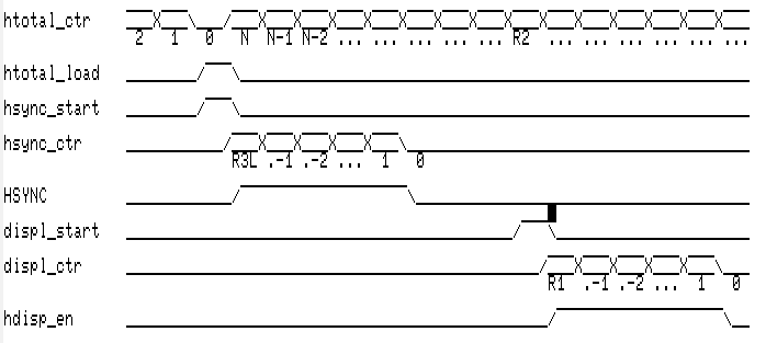 This is sufficient to generate, for example, a solid block on a display.
However, there's more that must be considered when looking at supporting
horizontal smooth scrolling.
The counter values above are in units of characters, not in pixels. Within
each character column, there are some number (configurable via the high half of
R22) of pixels, with 8 pixels being maximum. This character dot counter is
also a down-counter, as far as I can tell from the available documentation.
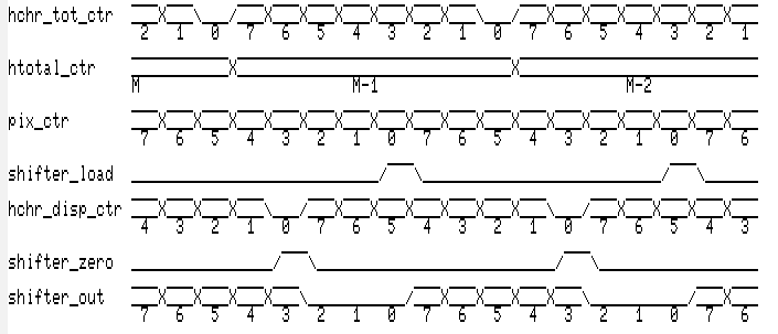
Thus, we expect to find timing similar to this (assuming 6 pixels per character
cell):
 (If you've ever wondered why the VDC keeps asking you to subtract 1 from things
here, and add 1 to things there, this is why. This is also why you must
reprogram the sync generation registers whenever you change the number of
pixels in a character.)
In order to support smooth-scrolling, however, we need yet another counter.
This one is programmable from the lower half of R25. When this counter reaches
zero, then we know to reload the pixel shift register. Based on how the
character data is laid out in the VDC documentation, the shifter always draws
its video data from the most-significant bit of the bitmap byte; in other
words, bit 7 is always shifted out, then bit 6, etc. for as many bits as is
configured to exist in a character cell.
 I think the original VDC would have also used shifter_load to trigger a memory
fetch for the next character as well. It'd involve three fetches:
1. Fetch the next character matrix byte.
2. Fetch the next attribute matrix byte (if attributes are enabled).
3. Fetch the character font byte for the character fetched.
Assuming these fetches take one dot-clock to complete, that implies that the
minimum character width is 3 pixels if attributes are enabled; 2 otherwise.
Since the VDC-II is intended to work with modern memory architectures, which
strongly favors streaming over random access, it will work a bit differently.
The assertion of the HSYNC pulse will trigger a sequence like the following:
1. Fetch the next HDISPLAY character matrix bytes into a holding buffer.
(Bad-line only.)
2. Fetch the next HDISPLAY attribute matrix bytes into a parallel holding
buffer. (Bad-line only.)
3. For each byte fetched into the character holding buffer, fetch the character
font byte for the named character into a line buffer.
It's regrettable that I'll need a bad-line mechanism, but that is a constraint
put on me by external factors that I have no control over.
Getting back to the smooth-scrolling support, remember that characters can have
fewer pixels displayed than exist in the font data. Here's a hypothetical
situation that we find in the Commodore 128 Programmer's Reference Guide: 5
pixels per character but an 8 pixel character cell width. We might want to
have another display enable signal that operates on a character column basis.
Alternatively, and I think this is most reasonable, command pulses that zeros
the shift register (which has the same effect as a dedicated enable).
According to the VDC docs, if your character cell is wider than the number of
pixels in a character, then to smooth scroll, you not only adjust the
smooth-scroll register, but also (strangely) the horizontal character display
total register as well (bottom half of R22). In the example above, R25 would
be set to 4 (which is why pix_ctr is 4 after restarting the character
boundary), but for some reason, you want to set the character total register to
1. Why is that?
It's never explained in the PRG; but, the reason appears to be that the
character display total and horizontal smooth-scroll registers are both
synchronized against the character total register reaching zero. At the start
of a character cell, the character total counter (yup! Another counter!) is
set to the horizontal character displayed value (R22), and counts down. When
that counter reaches zero, we negate the character display enable/zero the
shift register.
 So, in this bit of rambling, I think I've satisfactorily figured out how to
implement horizontal smooth scrolling in a manner compatible with the original
VDC chip, and explained why the registers behave as they do. It's definitely
not how I would have designed the hardware, but at least I now have an
understanding of how to implement more of the VDC-II's logic.
First HSYNC Pulse!!
04/18/2020 at 16:53
After installing the new 74LVC8T245 level shifters into the circuit and
reprogramming the FPGA to drive the DIR pin (which I've labeled A_B, because I
can never remember which side of the bus is driving when it's high or low), I'm
happy to report that the RC2014 booted fine.
I dropped into MBASIC from CP/M, and typed the following:
OUT 110,0:OUT 111,99
OUT 110,2:OUT 111,87
OUT 110,3:OUT 111,12
OUT 110,22:OUT 111,&h78
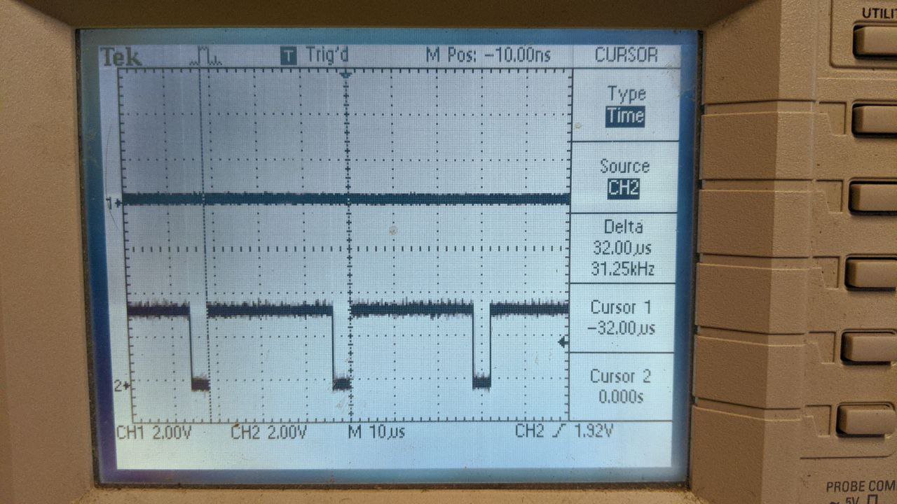
First line tells the VDC-II that there are 100 characters in a complete
scanline. The second tells the VDC-II where the start of the HSYNC pulse
resides on the scanline. The third sets the HSYNC pulse width. Finally, the
fourth tells the VDC-II that there are 8 pixels per displayed character with no
inter-character fill.
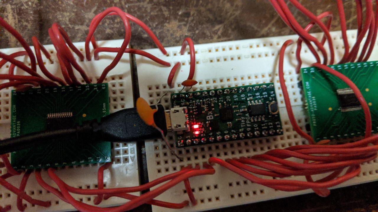
And I was immediate greeted with the following display on the oscilloscope:
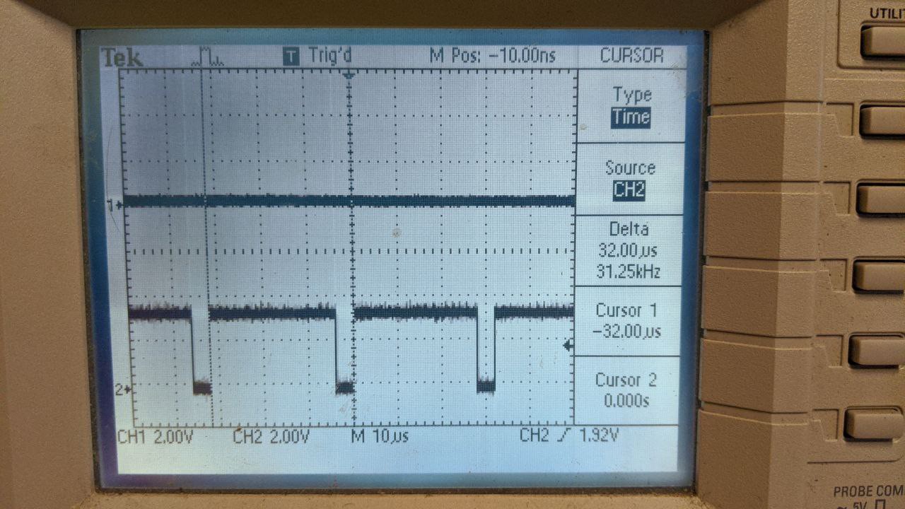 This tells me several things all at once:
1. You can interface to a Z80-compatible bus using 3-flop synchronizers clocked
at 3.3x the Z80 bus frequency, without needing a dedicated bus clock input.
2. TXS/TXB-type level shifters are not the correct type of level shifters to
drive any kind of real bus, backplane or otherwise. They seem to be most
useful for point-to-point circuits only; but, then, those are exactly the kind
of links where not having a direction control is not a useful advantage to
have. It's not clear to me what market TXS/TXB level shifters are intending to
penetrate.
3. 74LVC8T245 chips are powerful enough to drive a Mack truck, and fast enough
to keep up with a Ferrari. Just make sure you set the DIR pin correctly.
4. I really can solder SMT components without specialized equipment.
5. nMigen rocks. TinyFPGA BX rocks. Based on my experiences with these tools,
you can bet I'll try building more ambitious projects with this gear in the
future.
74LVC8T245PWRs Have Arrived
04/14/2020 at 15:36
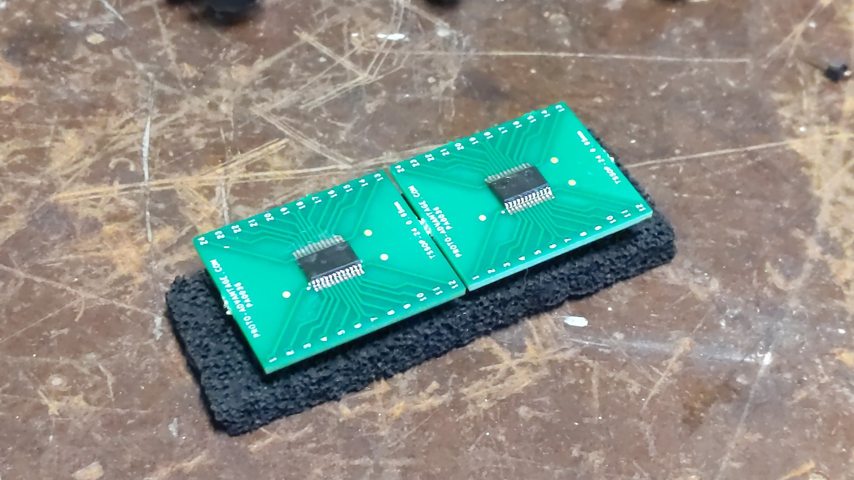
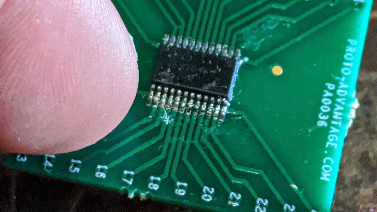
My collection of 74LVC8T245PWR chips have arrived. These are 24-pin TSSOP
chips which I had to build my own break-out boards for. That was frustrating
(especially as I'd never soldered SMT parts before); but, I was nonetheless
successful. Continuity checks indicates no bridges, shorts, or open circuits,
so these ought to work out nicely.
I've already updated the circuit schematics to include these new chips in the
design. I lost steam after rendering the schematics, but hoping to wire them
into the circuit this-coming weekend.
 Still Waiting ... In the Mean Time...
04/06/2020 at 15:39
While I wait for the 74LVC8T245 chips to arrive, which seems like it'll be
forever thanks to a certain virus, I've decided to try and use my spare
TinyFPGA BX as a test harness for the VDC-II.
This means resurrecting the Kestrel-2, but in a reduced form, as the TinyFPGA
just doesn't have the same resources that the Nexys-II's FPGA (Spartan 3E as I
recall) has. The first step towards targeting this chip, though, is rewriting
the CPU into nMigen, a process which I've already begun and hope to finish
soon.
Z80 Bus Interface Works . . . Maybe.
03/30/2020 at 04:30
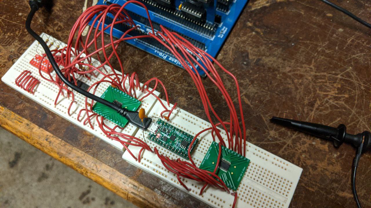
After building the initial circuit for the VDC-II "chip" (a TinyFPGA BX
programmed with the VDC-II core in progress), I was greatly disappointed to
learn that it did not work once I placed the FPGA in-circuit. Until that
point, everything worked great. But, once the FPGA was in-circuit, the level
shifters started to behave with wild abandon. So much so, in fact, that the
RC2014 computer I'm using refused to boot.
The data bus had wild, 50-52MHz oscillations on them, crazy amounts of
overshoot and undershoot at times, and you can clearly see where the one-shot
circuits of the level shifters would start and stop. All in all, the logic
levels were not clean, and I'm convinced the Z80 and/or memory on the bus
refused to have anything to do with this nonsense.
Here's the schematic (PDF) of the current circuit.
After taking the TinyFPGA BX out of the circuit, I decided to just test it by
hand, the good old fashioned way: strap a bunch of pull-down resistors on all
inputs, and selectively use wires to +3.3V to raise them high when needed. I'm
happy to report that, as I type this, the VDC-II core (such as it is) seems to
be able to accept and return bytes via the Z80-side of the interface.
In theory, I could have programmed the chip sufficiently to actually start
generating an HSYNC signal. However, I didn't bother going this far;
manipulating the bus interface by pulling and setting wires in the breadboard
was terribly exhausting on its own. Maybe tomorrow; or, I'll just wait for the
new level shifters to arrive instead.
## Miscellaneous Images and Videos
In no particular order...
 Video of VDC-II In Action (YouTube)
 As I type this, there are still some bugs to be worked out. While editing
the fat-bits view of a character, the display gets corrupted for some reason.
I'm still trying to work out why this is. However, it does not crash the
software, and it legitimately does update the correct glyph bits, which you
can confirm by dismissing the Glyph Editor and re-opening it.
Also missing is the ability to load or save data from/to a file. This will
be coming soon enough. I'd like to get the basic program functionality
working first.
Anyway, just a reminder that I'm not dismissing this project; my professional
obligations have been taking more than a fair amount of my bandwidth. I
can't wait to be able to run this software on real hardware though!!
Work, work, work, ...
06/13/2021 at 19:43
What happened?
Well, I got a full-time job for a major manufacturer of mass media storage,
so that's been occupying most of my time.
Finally heard from Crowd Supply about a month ago that they're still waiting
for parts to complete my order for TinyFPGA BX modules. Who knew the
semiconductor shortage would take out the BX-Plorer project?
Still, I've not had two seconds to rub together to hack on the VDC-II HDL
code. Which sucks, because I am itching to make some progress with it. I
desperately want to finish it by end of this year, so I can move on to other
things.
But, now that I'm starting to get into a routine at my day-gig job, I'm
hoping to re-allocate some weekend time to get back to work on the Font
Editor code for the VDC(-II), and subsequently to that, to actually finish
the VDC-II itself. I would love to be able to get CP/M running natively on
it using my RC2014.
Adulting is hard. Avoid becoming an adult if you can.
VGA PMod Adapters
01/14/2021 at 00:53
I ordered some VGA PMod adapters from Digilent last week, and I'm happy to
say that they fit perfectly. The mechanical connection is very solid, far
better than any card edge connector I've used. Near as I can tell, the
electrical connection also seems to be good as well.
I haven't had the chance to reprogram the FPGA design to use this particular
adapter yet. I will update with my results upon completing that.
 The only thing which sticks out to me, besides the height of the connector,
is ... the height of the connector. And, its orientation. But, if you can
strain-relief the monitor's cable appropriately, it should not pose a problem
for the BX-Plorer.
(Aside: my experience with how well this PMod fits into the sockets on the
BX-Plorer has convinced me that the right way forward for the Kestrel-3's
backplane should be 2x40-pin RC80-compatible connectors.)
Crowd Supply, More Parts on Order, Etc.
01/09/2021 at 21:42
Now that I have what I believe to be a functioning prototype of the BX-Plorer
design, I have reached out to Crowd Supply to see if they think this project
is worthy of crowd-funding and selling through their website. So far, after
about a week of waiting, I have not heard anything back from them. Their
website does not provide any indication of how long I should have to wait for
an answer. I've opened a support ticket with C/S as well, but again, no
response. If C/S doesn't respond within another week or so, I shall start
looking into selling my kits elsewhere.
In the mean time, I have placed an order for three Digilent PMod VGA adapters.
(Three, because these things are easy to lose!) Although these adapters
support 4 bits per gun (and, thus, support 4096 colors maximum), I can only
use 3 at the moment because of my previous wiring mistake. Still, it should
work for the purposes of demonstration.
Another thing I'd really love to hear back from C/S about is my outstanding
order for five more TinyFPGA BX modules. Back in December, they said that
they expect a new shipping date some time in January. I sure hope they
haven't forgotten about me. I'll give them until February before I contact
them again about my order.
While waiting for all this stuff to work itself out, I've been making
progress on the font editor demo. Here's the latest screenshot (taken off a
Commodore 128 emulator), and is a good representation of what it should look
like on an RC2014 with a VDC-II card as well. I still need to write the code
to render all the characters inside the table cells, to scroll the glyph
palette table up and down as appropriate (to allow selecting any of the 512
supported characters), and of course, the actual editor interface as well.
Still, progress is progress.
 Revision 6A boards here; work great.
01/02/2021 at 07:31
Just before Christmas, I received the three prototype boards for revision 6A
from OSH. The boards look great, but I wasn't able to construct one until
yesterday evening.
 Assembly went ... not quite as smoothly as I'd've liked for the first board I
tried. It was a bit colder in the garage than I'd've liked, but the solder
hated it more than I did. While attempting to drag-solder the 74LVC8T245PWR
chips onto the board, no matter how much solder I used to flood the pins, it
refused to make a clean solder joint. Wicking the solder just wasn't working
well, so I tried to apply a bit more pressure. While that worked to get the
solder hot enough to wick, it also bent the pins of the chips, and ... yeah.
Lesson learned: do not drag-solder when your workspace is cold.
 (note the red lines showing where the pins got crushed together.)
After refining my technique to use tack-soldering instead, and making sure to
wick excess solder pulling away from the chip instead of trying to sop all
the excess in one fell swoop by dragging the wick across the pins,
construction went relatively smoothly. I completed the build of the 2nd
prototype card in about six hours.
 After fitting a TinyFPGA BX module to the card, I was able to use it as a
proper VDC-II card by routing wires over to a breadboard with a resistive DAC
on it.
 I ran the old clock demo I'd written some time ago, and it runs perfectly.
(A more advanced demonstration which puts the VDC-II into bitmapped graphics
mode is still under development as I write this.)
 Next steps include:
* Double-check and make sure the extra I/Os exposed by the new Rev 6A board
have continuity. If they do not, it'll be because of how I soldered the
connectors to the bottom of the TinyFPGA BX module, and not due to a wiring
issue on the 6A board. (I already checked the latter, and they seem to work
as far as I could tell.)
* Begin the process of seeking Crowd Supply feedback.
* Continue working on the VDC-II font editor tool. I've neglected to post
updates here mainly because I never seem to make big enough progress with it;
that, and I'm coding it on a Commodore 128 emulator for convenience. But, I
suppose I will start posting software updates here too, as eventually, this
software will be ported over to the RC2014. The VDC and VDC-II parts will
need somewhat different initialization logic, but once initialized, they
should behave identically. So, having the C128 version handy as a reference
implementation will be useful.
Notes on How To Solder Belly Connectors
12/03/2020 at 18:43
I have been thinking about how to reliably solder the surface-mount pin
headers to the TinyFPGA BX module for some time now. I think I've come
across a solution.
1. Solder on the 14-pin outer/through-hole connectors. It's important that
they be soldered for mechanical stability in later steps.
2. Insert two pins of the surface-mount pin header into female strip socket.
3. Insert the female strip socket cross-wise on the TinyFPGA's through-hole
pins.
4. Insert another strip socket a few pins away to lock in the registration.
5. Now you can solder the ends of the surface-mount connector to the board
with full confidence that they'll line up correctly with the socket on the
PCB.
6. Scoot the cross-wise sockets down, and solder the other end of the surface
mount socket.
7. Now you can remove the cross-wise sockets, and solder the remaining pins.
Here's a picture of a mock-up which demonstrates what the arrangement should
look like after step 4, but before the completion of step 5.
 Demo Software Project: Font Editor
12/03/2020 at 18:31
It has occurred to me that my plans to complete VDC-Forth are essentially
kaput; it is a user interface model for a Forth that I'd hoped would give me
some unique insights and inspirations, and instead I have essentially coded
myself into a corner with it. While I do intend on playing more with the code
in the future, it's not clear to me that it will remain my "go-to" piece of
software I can point someone to and say, "Look, here's code that works directly
with the VDC-II core you can study."
One thing that I will need in the future, though, is a font editor for this
module. So, I figured, why not write a font editor for it, using it? And, so,
that's what I'm doing.
It's written to use 640x200 bitmapped mode, monochrome. I chose this because
had I used text-mode, I couldn't easily alter the font heights. Remember that
the VDC chip supports fonts as small as 1 pixel tall and as tall as 32 pixels.
Since vertical sync timing is dependent on this height, every time I'd need to
alter the font height, I'd need to recompute (dynamically) the CRTC settings.
With this comes the risk of user-visible loss of monitor sync, which is
annoying to say the least.
So, bitmapped mode it is. So far, I've implemented code to draw horizontal
lines and draw filled rectangles using patterns. Although their APIs are quite
primitive and low-level, they work.
Just ... not very fast. I predict the issue is caused by needing to read from
and write to the VDC for every byte transferred. I could probably double
performance by only read-modify-writing the left- and right-hand edges of the
rectangles, and just blindly writing the interior bytes.
Even so, this software isn't intended to win any races, and certainly not to
race the beam in any way. So, correctness is the most important aspect of the
code. I might spend some time to optimize the code a bit, but I won't spend
too much time on it.
Now that I can draw nice rectangles and horizontal lines, the obvious next step
is vertical lines and, after that, text. Once that's done, I'll have the
ability to render the complete user interface for the font editor. From there,
actually implementing the editor proper should be relatively simple.
I think.
Source of Error Found
11/27/2020 at 23:38
So, why did I make such an egregious error when designing revision 5B boards?
Because the TinyFPGA BX project has (or, at least at one time, had) poor
revision control and misleading or missing documentation.
When I was building revision 5B, I was working off of this photograph, which is
one of the only documented listings of the I/O pins accessible on the underside
of the TinyFPGA BX module. (If you can find an official description of those
connectors on the https://tinyfpga.com website, please send me the link!)
Observe the bottom "belly connector" (what do you call those things anyway?) is
a 2x7 surface mount connector, which lines up with what I've built the 5B to
work with.
However, if you look at the current OSH Park PCB artwork, you'll see that
there's a 2x8 surface mount connector in its place. This matches up with the
actual hardware I tried using to build the latest prototypes with. As far as I
can tell, it looks like the exact same pin-out as the 2x7 connection, but with
an extra pair of ground pins.
Of course, looking at the schematic, I see that it describes the 2x8 connector;
but, considering the Crowd Supply updates are newer than the schematic up on
Github and showed the 2x7 connector, I didn't put much stock in trusting it.
Turns out, Crowd Supply's information is outdated. And, strangely, I can't
even find reference to the 2x7 connector in Github's history, suggesting that
the CS campaign started before the Github repo even existed.
So, yeah, I learned a lesson on this one: never trust the updates on Crowd
Supply. Even if newer than repository documents, they may not reflect current
reality.
OK, back to hacking on the next PCB revision.
Revision 5B PCBs are trash; need another revision.
11/15/2020 at 23:19
Rev 5B boards have a critical design failure. The "belly connectors" of the
TinyFPGA BX module has two parts: one is a 2x3 surface mount pin header, and
the other is a 2x8 surface-mount pin header. You can use a 2x7 pin header for
that connector; but it must be offset by 100mil in order to work.
Problem is, if you look at the PCB artwork, you'll see that the 2x8 belly
connector has only 14 pins. And, it's not offset. Which means that the whole
design is junk.
There are no work-arounds for this. I need to spin a new batch of PCBs with a
proper 2x8 belly connector. Sigh.
Upon inspection of the rest of the PCBs, though, everything else looks nice.
I'm particularly pleased with the host Pmod connector alignment. So, there is
that, at least.
Dammit, I really am getting impatient with this project, though. I'm spending
too much time waiting and burning through way too much cash.
Revision 5B Boards Completed
10/17/2020 at 22:10
I'm happy to report that I've completed work on yet another revision of the
BX-Plorer PCB, and this one even includes a logo and more prominently placed
revision and release date. Yay for professionalism!
Even more than that, I've managed to source the proper connectors to support
honest to goodness Digilent-compatible Pmod host ports! This allows a wide
variety of pre-existing Pmod-compatible attachments to be used with your
RC2014.
Test cards have been ordered from OSH Park. They should arrive in a few weeks.
I still need to place the orders for the rest of the components though. I
should be doing that later this-coming week.

 BX-Plorer: Meet the New Card, Same as the Old Card
10/08/2020 at 20:11
As this project evolves, I'm noticing a distinct yet synergistic
compartmentalization in the roles and responsibilities of different project
components. When I started this VDC-II project, I'd just been convinced by
interested members of the community of the value of developing Kestrel-3
computer parts for the RC2014 backplane. I later observed that my RC2014 Zed's
flash BIOS image could be built with Commodore VDC support, and after reading
up on that chip's technical specs, I realized that it was a fairly close match
to what I'd wanted to achieve with my own CGIA concept. So, rather than
re-inventing the video support with the CGIA, I figured I'd just piggy-back
what was already there, and decided to reimplement the VDC. This benefits both
RC2014 and Kestrel-3 communities, since any Kestrel-specific enhancements I
make to the design later on can benefit both communities, not just the one.
So, I set out to just develop a (mostly but not completely compatible) clone of
the Commodore 8563 VDC as used in the Commodore 128, using affordably priced,
off the shelf FPGA development boards. That became the VDC-II project you're
reading about now.
I've always intended to release this project as a kit of some kind, so that
RC2014 owners can, in long-standing RC2014 community tradition, build their own
video card. That means, as part of the kit, they'd receive the PCB, all the
chips, a pre-programmed TinyFPGA BX module, and other miscellaneous parts
needed to have a working video card.
However, I now realize that the very circuit I used to interface my TinyFPGA BX
module to the RC2014 backplane is itself useful as a self-standing product in
its own right. You could see a less developed realization of this, more or
less explicitly, in previous log entries where I first mention breaking up the
FPGA part of the circuit from a mezzanine card containing the analog VGA
circuit.
Going forward, I've decided to formalize the separation of the FPGA project
card from its applications. First, the FPGA project card now has an official
name: BX-Plorer. It lets the consumer of the card explore FPGA designs using
the TinyFPGA BX module.
Second, I've decided to factor the BX-Plorer out into a separate git
repository. I'll update my Hackaday.io configuration accordingly shortly after
making this post. This implies that, Coming Soon, there'll be a separate Git
repository for the VDC-II design files and the software stack needed to drive
it. I'll (re)post updated links in a separate log when everything is in place.
Related to the first two points above, for now, both BX-Plorer and VDC-II
updates will happen in this Hackaday.io project. As I write this, I have no
plans of factoring the two projects out here. These two projects have been
co-developed from the get-go, and I don't see that changing any time soon.
Third, what of the VDC-II-based RC2014 "video card"? Is that now dead? As I'd
originally conceived it, yes. With all the other video card projects that
people are concurrently producing for the RC2014 (link 1, link 2, link 3), it's
not clear to me how I can compete for mindshare. However, if there's enough
feedback, I can see offering a BX-Plorer Cost Reduced/Fixed Function card as a
dedicated video card. If this is something that is still desirable to readers,
please do get in touch to let me know.
(Besides, you can always use a regular BX-Plorer with a pre-programmed TinyFPGA
BX and analog VGA mezzanine still.)
Fourth, this does not affect the development of the VDC-II itself. I still
need a video card, for both my RC2014 and for my own future homebrew computer
design. The VDC-II project is not dead.
When, not if, you see these new terms being bandied about in my project
updates, now you'll know why and where they come from. :) Until next time!
Revision 5 Circuit Design Underway
10/08/2020 at 18:05
As I continue to read up on my responsibilities for working with Crowd Supply
(CS), I realize that, being a vetted interaction process, CS is almost
certainly going to call me out for not exposing all of TinyFPGA BX's I/Os. So,
I'm going to head that issue off now and work to expose all of the I/Os that
this module has to offer. This will in effect turn the card into a generic
FPGA development card. I'll mention more about this in a related but separate
project log update.
This is not as simple of a task as it sounds; I need to:
* create a new TinyFPGA BX schematic symbol.
* create a new TinyFPGA BX footprint for PCB layout.
* figure out how to expose all the I/Os.
* create revised schematics and PCB layout.
These steps took me about three days so far, and I'm still working to complete
the list. Here's a summary of the changes I've made to the design so far and
what can be expected from revision 5A boards.
First, the dedicated 2x7 pin socket that I'd intended to replace the 14-pin DIP
socket (in an unreleased revision 4B PCB design; you can see it in the Github
repo though) has been replaced by a set of three 2x6 pin sockets, spaced 0.9"
apart, and whose pinouts comply with Digilent's Pmod interface specifications
at 3.3V. I'm currently placing them across the top of the PCB for easy access,
as that's the only edge long enough to accommodate them. This brings 24 I/Os
out for general purpose use. There's a catch, though; these sockets are not
right-angle sockets. I intend these sockets to be used with Digilent's
12-conductor Pmod cables to attach devices to. The PCB is already big enough
to flop around in the RC2014's single row backplane socket, so you don't want
to put too big of a load on those sockets. Building a mezzanine card will
extend the height of the PCB, which will make it more floppy and less
mechanically sound than it already is. Cables can be routed, which enables
them to also act as strain reliefs. That said, if I can source through-hole,
right-angle connectors, they should be drop-in compatible, if you can find a
way to mechanically secure the contraption.
Second, I will bring out the 5 shared I/O pins to a 2x3 pin header. This
header will have a comparable pin-out to the TinyFPGA BX pin cluster. Being
that these will be exposed pins, you can connect to them using Dupont
connectors.
Between these two changes, the BX's remaining 29 I/O pins will be fully and
much more easily accessible to hardware hackers.
Revision 4A PCB Built, Works
09/24/2020 at 22:23
Just wanted to say that I finally completed building the revision 4A board;
most of the hardware was discussed in the previous log entry, but I've fitted
the '688 comparator for address decoding as well as the TinyFPGA BX module.
The result is shown in the pictures below.
I'm happy that, despite needing one bodge wire from U2 to +3.3V, it is
otherwise fully capable of working from the POV of software development.
I've already made the changes to the design files to support revision 4B, which
fixes all the known hardware bugs. Additionally, the nMigen files for the
VDC-II has been configured to output 9-bit video, so all 11 output I/Os are
known to work.
Besides getting revision 4B out the door, all that remains is a set of
mezzanine boards: one for VGA, and one for PS/2 keyboard and mouse. That,
combined with a reasonable GEOS-like GUI system, should be sufficient to make
the RC2014 into a reasonably usable homebrew computer system.

 PCBs Received, First Build
09/18/2020 at 17:25
On the 14th, I received my printed circuit boards for the Pixel Pusher. Yesterday, I got around to trying to build one of the three prototype boards I received.
 This is what a bare board looks like, component side up.
 My first task is to place the highest risk components first, so as to just get them out of the way. In this case, the two 74LV8C245PWR chips, as they're incredibly small devices that even an idle breeze can cause to slip off and never be found again.
 I use blue duct tape for this purpose which is not the best thing to use but it's all I had available. Tacking one corner of the chip down is sufficient to hold it in place.
PRO TIP: The ideal tape for this would have been blue painter's tape. In order to reduce the stickiness of the duct tape down to something comparable to painter's tape, I just applied and removed the duct tape strip off the work bench several times until I was comfortable with the strength of the remaining glue. The workbench was naturally dusty, so each application added more dust to the strip, which had the effect of reducing how sticky the strip was.
 I next applied liberal amounts of solder to the chip's connections. This
ensured all pins were soldered to the pads, but it also ensured that all pins
were soldered to each other as well. This excess solder had to be removed. I
used solder wick for this purpose.
 After fighting a bit with the solder wick (as evidenced by the slightly
scorched flux residue), I sopped up all of the excess solder. Solder wick does
not remove everything, and it happens to work out that what remains is
sufficient to both hold the chip in place and to ensure good contact.
Because the contacts are so small, however, It is best to perform continuity
checks with other parts of the circuit. If you need to desolder and
resolder/reflow the contacts on these parts, now is the time to do it before
other components are added.
I just discovered that the 3.3V supply pin of U2 is not connected to the 3.3V
trace. I forgot to place a via! I'll need to add a bodge wire later.
 After repeating the steps above for the second level shifter chip, I'm left
with a board with two nicely soldered, surface-mount chips. Thankfully, I
didn't discover any more missing connections!
 I found out the hard way that the footprint used for the DIP switches (which
should have been a normal 14-pin DIP footprint) was too wide for the actual
switch. Thankfully, I could splay the legs of the switch out and make surface
contact with all the holes on the component-side of the board. Since all the
holes are fully plated through (per OSH Park's website and as continuity checks
confirm), treating the DIP switch package as a surface mount device instead of
a through-hole device provides the extra length needed to ensure good contact
with the rest of the circuit.
So, I splayed the pins out, tacked opposite corners of the DIP switch down,
and ...
 proceeded to blob solder on the remaining pins. I then set the DIP switches so
that the card will respond to I/O ports 6Eh and 6Fh (not shown). I then set
the DIP switches on the breadboard prototype to respond to I/O ports 6Ch and
6Dh, which would allow me to have both VDC-IIs in the RC2014 circuit at the
same time without contention.
 Next, I needed to fit a 28-pin, 0.6" wide socket for the TinyFPGA BX module.
However, I didn't have any on-hand. Disturbing; I believe I ordered these some
time ago via Amazon. Whatever, no biggie; I instead took a spare 40-pin socket
I had available and chopped off six pins on either side. The result fits
perfectly.
 More hackery was required, as I also found out I didn't have any 14-pin DIP
sockets handy either. So, I took another 0.6" wide socket (24-pin, in this
case) and performed surgery on it to produce two make-shift 7-pin SIP sockets.
I then placed them onto the PCB, and squeezed them together until they were
0.3" apart, roughly, which you can see below.
 Of course, this socket is not intended to seat any chips; rather, it was
intended to be used as the receptacle for a corresponding plug on a mezzanine
board which included the analog bits of the interface. See my previous log
entry for details on its pin-out (for video output purposes at least).
 After installing the decoupling capacitors, I finally now had the means to
install the bodge required to connect U2 to 3.3V supply.
This completes the soldering of the components onto the board. After soldering
the 40-pin plug onto the board, the finished result looks really quite good, I
must say.
 Here we see both the original breadboarded prototype of the circuit in the
foreground, and immediately behind it (the only purple PCB there), we find the
Pixel Pusher Revision 4A board sitting in the RC2014 backplane. These two
circuits are (as far as my checks can confirm) electrically identical, so once
I populate the Pixel Pusher card with a TinyFPGA BX and the 74HCT688 comparator
chip, it should "just work" (where "work" is defined as the card should match
the observed behavior, bug for bug and feature for feature, as the breadboarded
circuit).
I ran out of time to perform testing; so, I'll need to wait until later to see
how it performs.
Prototype PCBs ordered.
09/01/2020 at 23:53
That is all. ETA on delivery is September 11, but I probably won't get
around to assembling one until some time after that.
PCBs Designs Finished
08/29/2020 at 02:02
I've completed the initial design for the printed circuit boards for the RC2014
computer. This is my very first PCB design in KiCad, along with my very first
4-layer board, so I really have no idea what I'm doing. That said, I did it
anyway, and the first batch of printed circuit boards have been submitted to
OSH Park.
 Nothing has been ordered yet, however. I'm waiting to hear back from OSH's
support team on one question I had after uploading the designs. But, assuming
everything checks out, I'll be placing an initial order for three circuit
boards.
The circuit boards will make use of a 14-pin DIP socket as a connector for a
mezzanine circuit board. This connector provides access to 11 digital I/Os on
the FPGA, which is enough to drive an analog VGA port using discrete resistor
DACs. The pin-out of the J2 connector (as it's currently labeled on the PCB)
is as follows:
| Description | Pin | Pin | Description |
|-------------+-----+-----+-------------|
| R2 | 1 | 14 | R1 |
| R0 | 2 | 13 | G2 |
| G1 | 3 | 12 | G0 |
| GND | 4 | 11 | +3.3V |
| B2 | 5 | 10 | B1 |
| B0 | 6 | 9 | n.c. |
| HSYNC# | 7 | 8 | VSYNC# |
This pin-out supports a 512 color display. However, if you reprogram the FPGA
for other tasks, it can be used to, e.g., control SPI or I2C devices, and so
forth.
One pin is no-connect, and is intended to allow future mezzanine boards to
auto-detect which version of the connector they're plugged into. For example,
if a later revision of the video card supports 32768 colors, I'll need to add 6
more pins (at least). A 32K-color mezzanine designed for the 20-pin connector
can still plug into and inter-operate with the older 14-pin connector, if it
pays attention to pin 9. (Although, how it is to pay attention to pin 9
remains to be specified. YAGNI.)
Strip Buffers Done, VDC-II Core Usable (more or less)
05/30/2020 at 22:09
I've completed the strip buffer implementation, the block memory arbiter, and
the video fetch engine, and mated it with the MPE. This provides the host
processor the ability to manipulate the display memory and we can finally
observe the effects on the screen!
After setting the video mode to 80x30 text display, placing the text display at
address 0000H and the attributes at 0C00H, you can run this little program in
BASIC on the RC2014 to look at the first half of the VDC's character set
(glyphs 0 through 255).
1000 OUT 110,18:OUT 111,0
1010 OUT 110,19:OUT 111,0
1020 OUT 110,31:FOR I=0 TO 2399:OUT 111,(I AND 255):NEXT I
1030 OUT 110,18:OUT 111,12
1040 OUT 110,19:OUT 111,0
1050 OUT 110,31:FOR I=0 TO 2399:OUT 111,(I AND 15):NEXT I
BASIC is slow enough that you don't need to worry about waiting for the MPE to
finish stores into video memory; if you write this code in machine language,
however, you'll need to remember to wait on the VDC. In any event, it should
produce something resembling the following (if attributes are turned on).
 If you turn off the attributes and set the foreground and background colors to
bright green and dark grey, you'll get a display which kinda sorta looks like a
Commodore PET (or the Commodore 128 when it boots in 40-column mode).
Bitmapped graphics mode works as well. If you ran the previous code above,
then try executing the following listing, you should see high resolution
"garbage" on the screen, complete with color attributes applied. NOTE:
the TinyFPGA BX is only big enough to contain 16KB of video RAM, as that's all
the block RAM it has available. Thus, the 640x480 VGA display is going to have
several repeated slices showing the same data. That's normal and expected.
OUT 110,25:OUT 111,INP(111) OR 128
 Since the TinyFPGA BX only supports 16KB of RAM, there's no way to fit
attributes in with a full-screen bitmap image. So, you'd typically turn off
attributes to have a proper monochrome display. However, the VDC-II doesn't
yet support scan-doubling, so it renders the screen at full resolution whether
you like it or not.
OUT 110,25:OUT 111,INP(111) AND &HBF
OUT 110,26:OUT 111,&H51
 Interesting how you can see where the screen data resides, where the attribute
data resides, and where the character set resides in VDC memory. :)
So, now that I've demonstrated that I have a workable, usable display, I
figured it was time to try and write something that is "useful", in the sense
that it is representative of a typical program most would consider to be
useful. I decided to work on a simple clock application, and you can find
the latest source code to it in the repository.
Here's what it looks like when it first starts up.
 To unpause the clock, you tap the P key on the RC2014 terminal. It will then
start counting up, in roughly 1 second intervals. Kinda sorta like this:
VIDEO: RC2014 running VDC-II core on FPGA, Clock Demo
While working with the code, I ran into two hardware bugs. One of which I knew
about from earlier development; however, a new bug has manifested. The bugs
are:
1. If polling the status register too fast, it will corrupt subsequent MPE
operations. I've additionally discovered that this will even manifest when not
using block-copy or block-write mode. It can also show up as corrupted VDC
registers as well; it's not restricted to affecting video memory.
2. And the latest bug I discovered was that, for some reason, reading the data
register does not automatically update the update pointer. Thankfully, writes
to this register does not cause issues.
What's Next?
In no particular order:
1. Well, I'd like to finish the development of the clock; there are a few added
niceties I'd like to throw in.
2. I need to finish designing the printed circuit board for the VDC-II RC2014
card.
3. Implement missing features, like hardware cursor, row address increment
support, underline attribute support, etc.
4. Fix known hardware bugs.
Still a ways to go before I can declare this project "done"; however, it's now
certified to be in a usable state, which is quite exciting!
More Thoughts on Video Refresh
05/12/2020 at 16:22
The VDC video modes all assume that the VDC can access arbitrary video RAM with
impunity. While you can fetch character and attribute data sequentially,
resolving character codes to font data requires a potentially fresh hit to
video memory, starting at either BASE+(16*code) or BASE+(32*code), depending on
the configured character height.
Even if the character codes increase monotonically, the memory fetched will
have 16- to 32-byte gaps in between referenced bytes. This breaks the optimal
access pattern for synchronous memories, all of which are optimized for
sequential access patterns. A good rule of thumb for synchronous memories is
that every time you need to skip around in memory will cost you 10 cycles of
latency.
Although it is possible to sequentially fetch character and attribute data,
they occupy different segments of video memory, necessitating two video base
pointers and two processing engines. Correspondingly, if you fetch 8 bytes of
character data, you must also fetch 8 bytes of attribute data. The two bursts
of data must be synchronized with each other externally to the memory fetch
units.
Character and attribute bursts can happen in any order (e.g., attributes can be
fetched ahead of character codes), but they must always be adjacent. Moreover,
both character and attribute bursts must occur prior to font resolution, as
attributes provide the 9th character code bit.
On the iCE40LP8K I'm currently targeting, a ping-pong line buffer, such as what
I used to implement the MGIA on the Kestrel-2 and -2DX, will be prohibitively
expensive. The space for a single line buffer of 256 characters would require
2048 DFFs (and, thus, logic elements). We would need two of these, so that the
memory fetch logic can fill one buffer while the other is used for video
refresh. Note that the FPGA only has 7680 logic elements.
Because they switch roles only on HSYNC boundaries, full-line buffers must be
large enough to accommodate the widest display supported. The VDC-II register
space supports 256 characters (all 8 bits of R1 are significant). If we
couldn't accommodate a pair of line buffers large enough to support 256
characters, then we would need to ignore upper bits of register R1, which would
break 8563 VDC compatibility.
Video data (resolved character/bitmap data plus corresponding attribute
information) must be available when horizontal display enable asserts, since
that's when we must start shifting out video data.
All of these problems interact. Thankfully, besides the queue-based approach I
discussed in a previous log, there's another approach to work around these
matters.
Another Solution
Instead of using full-line buffers, we use a pair of ping-pong "strip" buffers.
Each strip is 4, 8, or 16 characters, depending mainly on externally imposed
video memory latency requirements. For the purposes of this description, let's
assume a 4-character strip.
A strip buffer contains two bytes for each character column it supports: an
attribute byte and a bitmap byte. When attribute data is fetched, only the
attribute bytes are updated. When character data is fetched, only the bitmap
bytes are updated. The interface presented to the dot-shifter logic, however,
always presents a 16-bit attribute/bitmap value pair.
To minimize the time needed to provide the complete set of data for a strip,
attribute data should be fetched first. That way, when character data is
fetched, we can stream data not only from video memory but also (in parallel)
the strip buffer to provide the complete 9-bit character code to the font fetch
unit. The font fetch unit can then resolve the character code to a bitmap
byte. For this to work, font data must reside in fast FPGA block RAM.
The following table illustrates the memory fetch access patterns with
0-wait-state memory on a pipelined Wishbone B4 interconnect to video RAM and an
asynchronous strip buffer read port. You could typically find this access
pattern when placing character, attribute, and font data in block RAM.
Assuming we reference video memory at the same speed as the dot-clock, we can
reload the strip with video data in just 13 pixels. Note that a four character
strip with 8 pixels per character contains 32 pixels, giving us ample time to
refill the strip buffer. Four characters at 3 px/char would have only 12
pixels, so we would expect to see visual artifacts under those conditions.
You'd want at least 4 px/char in order to ensure a clean display.
| Cycle | VRAM Address | VRAM Data | SBUF Read Address | SBUF Write Address |
|:------|:-------------|:----------|:------------------|:-------------------|
| 1 | ATTRPTR+0 | | | |
| 2 | ATTRPTR+1 | a0 | | ATTR0 |
| 3 | ATTRPTR+2 | a1 | | ATTR1 |
| 4 | ATTRPTR+3 | a2 | | ATTR2 |
| 5 | CHARPTR+0 | a3 | | ATTR3 |
| 6 | CHARPTR+1 | ch0 | | CHAR0 |
| 7 | CHARPTR+2 | ch1 | | CHAR1 |
| 8 | CHARPTR+3 | ch2 | | CHAR2 |
| 9 | FONT(ch0) | ch3 | PAIR0 | CHAR3 |
| 10 | FONT(ch1) | bm0 | PAIR1 | CHAR0 |
| 11 | FONT(ch2) | bm1 | PAIR2 | CHAR1 |
| 12 | FONT(ch3) | bm2 | PAIR3 | CHAR2 |
| 13 | | bm3 | | CHAR3 |
Below illustrates the same refresh attempt, assuming that both attribute and
character matrix data is located in a HyperRAM chip, while font data continues
to be confined to block RAM. In this case, we see it takes 23 pixels to reload
the strip buffer with video data, thanks to the HyperRAM access latency. As
you might imagine, four characters of 4 pixels each will not be sufficient to
refresh the display without artifacts. Therefore, if you intend on using a
character-mode display with narrow characters, you should strive to keep the
matrices inside VDC-II block memory space. Where possible, use external memory
resources only for bitmapped video modes, or, make sure to use sufficiently
wide characters.
| Cycle | VRAM Address | VRAM Data | SBUF Read Address | SBUF Write Address |
|:------|:-------------|:----------|:------------------|:-------------------|
| 1 | ATTRPTR+0 | | | |
| 2 | (wait) | | | |
| 3 | (wait) | | | |
| 4 | (wait) | | | |
| 5 | (wait) | | | |
| 6 | (wait) | | | |
| 7 | ATTRPTR+1 | a0 | | ATTR0 |
| 8 | ATTRPTR+2 | a1 | | ATTR1 |
| 9 | ATTRPTR+3 | a2 | | ATTR2 |
| 10 | CHARPTR+0 | a3 | | ATTR3 |
| 11 | (wait) | | | |
| 12 | (wait) | | | |
| 13 | (wait) | | | |
| 14 | (wait) | | | |
| 15 | (wait) | | | |
| 16 | CHARPTR+1 | ch0 | | CHAR0 |
| 17 | CHARPTR+2 | ch1 | | CHAR1 |
| 18 | CHARPTR+3 | ch2 | | CHAR2 |
| 19 | FONT(ch0) | ch3 | PAIR0 | CHAR3 |
| 20 | FONT(ch1) | bm0 | PAIR1 | CHAR0 |
| 21 | FONT(ch2) | bm1 | PAIR2 | CHAR1 |
| 22 | FONT(ch3) | bm2 | PAIR3 | CHAR2 |
| 23 | | bm3 | | CHAR3 |
As long as the strip is wide enough to support the longest latency of the video
memory, then we simply switch strip buffers after rendering the last pixel of a
strip. Switching strip buffers should also commence fetching the next strip's
worth of video data as well.
This algorithm should work to keep the video data sequenced for video refresh
while it is in the middle of the scanline. The next issue to tackle is how to
sequence the *first* strip, along the left-most edge of the display. The CRTC
doesn't have enough information to trigger the first strip fetch exactly 4-16
characters ahead of the left edge of the display. The only events we can rely
upon for this is:
1. The negation of the display enable signal.
2. The assertion of HSYNC.
3. The negation of HSYNC.
I believe each of these events would serve a unique role. We would accumulate
the address increment value to the fetch pointers when display enable falls.
We would schedule the first strip fetch at the assertion of HSYNC.
Bitmap mode can be implemented by simply not resolving character codes into
font bitmaps. "Monochrome mode" (that is, where one turns off attributes) can
be implemented by having the attribute fetch logic just synthesize default
attribute values based on register settings.
Thoughts on Handling Video Refresh
05/09/2020 at 01:14
At first, I thought the best approach to handling video refresh with the VDC-II
core was to use ping-pong scanline buffers, like how the Kestrel-2's MGIA core
did its video refresh.
I think that's still an approach that could work; but, I have to wonder if it
wouldn't be simpler to just use a collection of modestly-sized queues instead?
At its core, a video controller consists of two parts: the timing chain (which
I've already completed) and what amounts to a glorified serial shift register.
By its very nature, getting data from video memory to the screen happens in a
very pipelined fashion. Everything is synchronized against the dot clock, and
usually, also a character clock. Competing accesses to video memory, however,
could cause a small amount of jitter; perhaps enough to cause visible artifacts
on the display. Queues would apply naturally here, and can smooth out some of
that jitter.
The disadvantage to using queues, though, is that video RAM access timing is
much more stringent than with whole-line ping-pong buffers. I can't just slurp
in 80 bytes of character data, 80 bytes of attribute data, and then resolve the
characters into bitmap information (totalling 240 memory fetches), then sit
around until the next HSYNC. I will need to constantly keep an eye on the
video queues and, if they get too low, commence a fetch of the next burst of
data.
The disadvantage to using ping-pong buffers, though, is a ton of DFFs and logic
elements will go into making up the buffers. Like, if I want to support a
maximum of 128 characters on a scanline (128 characters at 5 pixels/character
can also provide a nice 640-pixel wide display), I'll need 384 bytes worth of
buffer space: 128 for the character data, 128 for attribute data, and another
128 for the font data for each character on that particular raster. 384*8=3072
DFFs, and if memory serves, I think you need one LE per DFF. There are only
7680 LEs on the FPGA. I can't use block RAM resources because those are
already dedicated for use as video memory (in this incarnation of the project,
at least; I'll work on supporting external video memory in a future design
revision).
So, while it's possible to implement a design using ping-pong buffers, it would
make very inefficient use of the FPGA's resources. Since logic would be strewn
all about the die, it could also introduce sufficient delays that the circuit
fails to meet timing closure.
The more I look at things, the more I think using a set of fetch queues makes
sense. I'm thinking a design similar to this would work:
 Key:
* CDQ -- Character Data Queue
* CAQ -- Character Attribute Queue
* BDQ -- Bitmapped Data Queue
* BAQ -- Bitmapped Attribute Queue
Of course, I'm still not quite sure how to handle bitmapped graphics mode. The
most obvious approach (which isn't always the best approach!) is to configure
the font fetch driver to just pass through the data. But, this will require
some additional though.
16KiB Video RAM, CPU Data Port Finished
05/08/2020 at 05:52
I'm happy to report some progress made on the VDC-II project. I finished the
CPU-to-video RAM interface. This includes block write and block copy functions
from the original Commodore 8563 VDC chip. Only one small problem...
If you try to use the VDC-II chip as documented by Commodore, where you poke a
register address, then wait for the chip to be ready, then poke a data value
into a register, the DMA engine (what I call the Memory Port Engine, or MPE)
corrupts video memory during a block operation.
However, if you poke the address, then poke the data, then wait on the ready
flag, everything works perfectly! This breaks backward compatibility with
Commodore's VDC, which makes me sad. It should work both ways; but, at least I
have a viable software work-around.
Next steps are to implement the video fetch logic and the memory bus arbiter
that will keep the different modules from stepping on each other's toes. If I
can fix the aforementioned bug, that'd be great; but it's not a priority for
me.
Can a VDC-II Support a 8K Display?
04/27/2020 at 01:54
I got an interesting (if not to be taken seriously) question on my Mastodon
feed today: 8K VDC-II when?
For now, let's focus exclusively on the CRTC capabilities, and completely
ignore the logistics of getting pixels onto the screen. The latter
implementation details will necessarily have to change regardless, so I take it
as a given that the VDC-II as I'm currently envisioning it cannot support
anything greater than a 1K display.
So, let's look at what the current VDC-II's CRTC registers can do, in regards
to 8K, 4K, 2K, and 1K displays, respectively. (By comparison, a 640x480 VGA
display is 0.8K.)
The Original Question: 8K VDC-II When?
I'm pretty sure the CRTC interface of the VDC-II will need to be changed to
support an 8K display. An 8K display resolution seems to be 7680x4320, at
least that's what Wikipedia tells me. The VDC-II CRTC supports a maximum
character cell width of 16 pixels; 7680/16=480, which is too wide for the 8-bit
horizontal displayed register to hold on its own. Thus, the VDC will need
either adjunct registers or an all-new 16-bit interface to cope with the
additional bits needed for horizontal timing.
So, at present, the VDC-II is not able to handle 8K displays. Sorry. It
probably can be made to support these large resolutions with relative ease;
but, it'll require more investment in the hardware description, an FPGA fast
enough to cope with the insane dot clock speeds, and testing with compatible
display hardware.
What about 4K Displays?
It's so close! While the vertical resolution is achievable with relative ease,
the horizontal direction proves to fall just short of the minimum required
functionality.
A typical resolution for a 4K display with consumer hardware is 3840x2160, so
I'll use that for my calculations. 3840 can be divided into 256 characters at
15 pixels each. The VDC-II, as I've currently defined it, does not support 256
characters; it only supports 255. However, a revision can be made to the
hardware description where plugging a 0 into the horizontal displayed register
(R1) could be interpreted as meaning 256 characters. It would require
redesigning the display-enable circuit to be a bit more clever than "assert
display enable as long as the display counter is non-zero."
The bigger problem is the horizontal total register (R0), which is used for
HSYNC timing pulse generation. This requires more than 256 characters; if you
think about it, the 256 characters discussed above are those which are the
visible part of the display. So, unfortunately on this basis alone, the VDC-II
cannot support a 4K display.
Things are a bit better in the vertical dimension, however. At 2160 pixels, we
can reasonably fit 216 10-pixel tall characters on the screen, 135 16-pixel
tall characters, or 108 20-pixel tall characters. All of these configurations
are well within the realm of possibility for the current VDC-II design.
What about 2K, then?
2K video is a different matter. According to Wikipedia, the largest recognized
2K resolution is 2048x1080. From the point of view of the VDC-II's current
CRTC implementation, this resolution is a cake walk.
With 16-pixel wide characters, the horizontal displayed register would be set
to 128, which (if you follow the rule of thumb that active video takes 75% of
the horizontal display time) means the horizontal total register would probably
be somewhere in the vicinity of 170. These are all easily within the range of
the 8-bit character counters as currently found on the VDC-II.
Similarly, in the vertical dimension, we're looking at a vertical displayed
setting of 135 (for an 8px tall font), 90 (for a 12px tall font), or 67 (for a
16px tall font). Note that the CRTC supports up to 32px tall fonts.
What Else is Needed?
One problem with 2K displays and higher is the need for 16-pixel wide fonts.
Commodore's VDC only supported 8-pixel wide font data. I wasn't planning on
supporting double-width fonts until I had a real need for them, but it is (as
can be seen above) a pretty obvious extension that can be made to a future
revision of the VDC-II core.
Obviously, with increased resolution comes the need for increased numbers of
bits to hold the required numbers. Horizontal total and displayed registers
are 8-bits wide presently. To support 8K, they'll need widening to 10- and
9-bits, respectively. It's possible similar expansion will be needed for the
vertical direction as well.
It's unknown how wide the sync widths (in either axis) are for these video
modes, so it's conceivable we'll need to add more bits to hold that information
as well.
Finally, you'll need enough video memory to support your preferred display
mode. Assuming a 16x16 pixel font for an 8K display, character mode screens
will take up 259.2 kilobytes just to hold the character and attribute data!
Contrast that with the VDC's original memory compliment of 16KiB (64KiB
possible). Moreover, the font data alone will need to be 16KiB in size for 8-
to 16-pixel tall fonts, and 32KiB for anything bigger.
Conclusion
Is it technically feasible that a VDC-II can be synthesized to support an 2K,
4K, or 8K display? Yes! These are not insoluble problems, and perhaps
surprisingly, very little resources are required to pull it off. The biggest
concern will be in how the VDC-II fetches from memory, how the advanced
features are exposed in the CPU-visible register set, and in supporting the
breakneck speeds required for these high resolutions.
But, will I be the one to produce a VDC-II that can support an 8K movie theater
display? Almost certainly not. Sorry!
CRTC Finished; First Pixels Displayed
04/26/2020 at 16:41
Treating the VDC as a superset of the 6545 CRTC chip has finally allowed me to
complete both the horizontal and the vertical sync generators. Additionally,
both generators use the same subcircuit description. You can see how I
configure two instances of the SyncGen class to work together in the VDC module
file.
After getting the sync generators working and bug-fixed, I was able to hook the
RGBI outputs to various internal signals to see what is happening. It was at
this time that I wired up my first resistive DAC as well.
First, I hooked the RGBI outputs up to the vertical sync generator's character
counter, to display horizontal color bars. At first, the colors were
distorted; I thought that my resistor values were off (I just grabbed the
closest values I could find to the ideal resistors). But, after fixing the
hardware description to account for the display-enable signal, the colors fixed
up nicely. Lesson learned: even though an LCD doesn't sling electrons at a
phosphor like a CRT, you still need to blank the outputs so that the monitor
has a proper black reference level.
 (without blanking the video)
 (with blanking the video)
For funsies, I then rewired the RGBI outputs to show the horizontal character
counter next.
 Finally, I decided to show the "character matrix" of the VDC output by tieing
the red signal to the HSYNC generator's xclken output, and green to VSYNC's
xclken output. The playfield will be illustrated by driving the intensity
output. This results in a nice graph paper-like effect and it visually shows
how several of the VDC registers interact. It's really neat to play with!
 (80x30, using 16-pixel tall characters)
 (80x60, using 8-pixel tall characters)
Sharp-eyed viewers might notice one final bug that needs squashing: notice the
top row of characters is elongated? That's because the vertical total adjust
circuitry does not negate the display-enable signal while operating. This is a
very simple fix to implement.
BASIC Program to Initialize the CRTC
This program initializes the VDC's CRTC registers to produce an 80x30 character
matrix display.
10 DATA 10
200 DATA 0,99
201 DATA 1,80
202 DATA 2,82
203 DATA 3,&h2C
204 DATA 4,31
205 DATA 5,13
206 DATA 6,30
207 DATA 7,31
209 DATA 9,15
222 DATA 22,&h78
1000 READ N
1100 FOR I=1 TO N
1200 PRINT I
1300 READ R,V
1400 OUT &H6E,R
1500 OUT &H6F,V
1600 NEXT I
To produce an 80x60 display, change these lines:
204 DATA 4,64
205 DATA 5,5
206 DATA 6,60
207 DATA 7,61
209 DATA 9,7
So, what of things like horizontal and vertical smooth scrolling?
Sorry to say; but, these features will need to be considered at a later time.
Evidence now shows that Commodore engineers implemented these features outside
the CRTC logic, so I'll have to also figure out how to do the same.
What's Next?
Right now, I think my next step is to implement the 16KB of memory needed to
hold a character matrix or bitmap display, so that I can use that to start
slinging pixels onto the display. This means I'll need to implement the
infamous "busy" flag, along with registers R18, R19, and R31.
VDC Vertical Sync: One More Chance
04/24/2020 at 14:45
I stumbled recently upon the data sheet for a MOS 6545 CRT controller and
MC6845 CRT controller chips. I noticed that the vast majority of the
sync-related registers map identically to those found in the 8563 VDC, which
leads me to believe that the 8563 has a 6545 buried within it. So, if I start
out building a 6545 clone first, I should be able to build the VDC in terms of
the 6545.
Most importantly, the datasheet provides the timing diagrams I needed to
understand how the vertical total adjust and such works, as well as how the
internal counters work. H and V character counters are up-counters as far as I
can tell, while "display" counters seem to be down-counters. All these extra
counters I was needing appear to be functionality that is VDC-specific, and not
CRTC-related at all. This is good to know, because I can factor functionality
into more manageable pieces.
So, before I replace the VDC's CRT controls with those from the CGIA, I'll give
the VDC one more chance, now that I know the foundation on which the VDC is
built and have a datasheet for the 6545.
(I still think it's overly complicated, and I still think the CGIA's approach
is simpler. However, I'd prefer to maintain as much compatibility as I can.)
Breaking Compatibility: HSYNC and VSYNC on VDC is Intractible
04/23/2020 at 21:37
I'm seriously thinking about just throwing away the existing HSYNC circuitry, and switching from a character-column-based system to a pixel-addressed counter arrangement.
There are several events that need to happen along any given axis of a display:
| Event | VDC Register (Horizontal) | VDC Register (Vertical) |
|:-----------------|:----------------------------------|:----------------------------------------|
| Blanking Starts | R35 (Display Enable End) | No equivalent |
| | R22H (Horizontal Character Total) | |
| | | |
| Sync Starts | R0 (Horizontal Total) | R4 (Vertical Total) |
| | R22H (Horizontal Character Total) | R8 (Interlace Control) |
| | | R9 (Vertical Character Total) |
| | | |
| Sync Ends | R3L (HSYNC Width) | R3H (VSYNC Width) |
| | R22H (Horizontal Character Total) | R5?? (Vertical Total Adjust) |
| | | R8 (Interlace Control) |
| | | NOTE: R9 ignored here! |
| | | |
| Blanking Ends | R34 (Display Enable Start) | No equivalent? Or, R5? (I can't tell) |
| | R22H (Horizontal Character Total) | |
| | | |
| Playfield Starts | R2 (Horizontal Sync Position) | R7 (Vertical Sync Position) |
| | R22H (Horizontal Character Total) | R8 (Interlace Control) |
| | | R9 (Vertical Character Total) |
| | | |
| Playfield Ends | R1 (Horizontal Display Total) | R6 (Vertical Displayed) |
| | R22H (Horizontal Character Total) | R8 (Interlace Control) |
With the 8563/8568 VDCs, these events are encoded in a variety of registers
which, frankly, make no sense and makes for hardware which is significantly
more complicated than it needs to be. It has taken me several weeks worth of
study and a corresponding amount of experimentation with emulators to finally
understand how to implement a compatible HSYNC generator, and to figure out how
horizontal scrolling would work.
I've been trying to figure out a corresponding theory of operation for the
VSYNC generator, but to no avail. It seems to defy any rational explanation.
Despite the registers seeming to indicate they are common circuits under the
hood, it turns out that there's enough minute edge- and special-cases that
differ between HSYNC and VSYNC generation that they each would require their
own formal specification.
I'm not sure I want to go down this rabbit hole.
It is especially weird that the VDC has separate registers for controlling
blanking along the X-axis, but not on the Y-axis.
Contrast this with my CGIA concept, which I'd intended for use with the
Kestrel-3 project. It uses pixel/line up-counters and magnitude comparators to
trigger events. Horizontal control circuitry always works in units of pixels.
Vertical control circuitry always works in units of raster lines. Both have a
similar set of registers. No exceptions, and thus, no strange surprises.
Plus, this approach directly supports features like raster interrupts, which
are notably absent on the original VDC.
The other criticism I have of the VDC approach is its extreme reliance upon
down-counters for almost everything, key word being "almost." In both X- and
Y-axes, there are separate down-counters for specific purposes (e.g., to
control the horizontal display enable, for example), but up-counters for other
purposes (e.g., vertical smooth scroll depends upon a down-counter, but knowing
which raster line to fetch for character font data depends on a corresponding
up-counter that holds the same information.) This is incredibly wasteful of
resources, to say nothing of how confusing it is to keep the design in your
head.
In conclusion, although I'm satisfied that I've been able to figure out HSYNC
behavior, I'm simply not able to crack the VSYNC behavior nut. I've spent
weeks on this problem, but haven't gotten any further than defining how the
display is generated without support for vertical smooth scrolling or the
vertical total adjust. Without a coherent method of generating HSYNC and
VSYNC, we can't get a stable display. For this reason, I'm deeply inclined to
change the programming interface for the VDC-II away from VDC-style CRT control
and replacing it wholesale with CGIA-style CRT control instead.
I really, really wanted to maintain backward compatibility with the VDC on this
particular aspect. But, I see that is proving to be more expensive in terms of
my time than I had hoped. Perhaps some external contributor can provide a
compatible hardware definition in the future. For now, I think going with the
CGIA CRT controls is the right choice for me.
Thoughts on Supporting Horizontal Smooth Scrolling
04/19/2020 at 21:41
Ever wondered why the C128's VDC has such a strange way of supporting smooth
scrolling? I did, and I'm sure I'm still wrong, but I think I've gotten pretty
close to the truth. Especially as my goal with VDC-II is to maintain backward
compatibility where it makes sense.
What follows is a brain-dump, me rubber-ducking with myself, on this very
topic. Enjoy! While working on the VDC-II's generalized sync generator
circuit, I realized that I needed to think about how smooth scrolling works.
This project log aims to record my current thoughts about how the 8568
implements this feature. DISCLAIMER! This information is hypothetical, even
speculative in nature, based on the documentation found in the C128
Programmer's Reference Guide and on observations of how VICE and the Z64K
emulators behave when I twiddle VDC register bits. I still don't have actual
hardware to test with.
Let's focus on horizontal smooth scrolling, since it's actually the *harder* of
two axes to consider.
It all started when I started to focus on the horizontal sync position register
(R2). It became clear to me that the horizontal total register (R0) is the
reload value of a down-counter. The HSYNC pulse down-counter is reloaded (with
the lower 4 bits of R3) when the horizontal total down-counter reaches 0, while
also also reloading the down counter with the value in R0. (In case you're
wondering, the HSYNC pulse is asserted as long as the horizontal sync
down-counter remains non-zero.) When the value of the horizontal total
down-counter is equal to the value in R2, *another* down-counter is reloaded
with the horizontal displayed value (R1). As long as the horizontal displayed
down-counter remains non-zero, a horizontal display enable signal remains
asserted. This is how the VDC knows where the playfield appears on the screen,
and how it can assert its borders.
The following timing diagram helps illustrate what I've discussed above.
Signals in all-caps are signals you'd expect to find exposed to another
circuit; lower-case signals are implementation details to the sync generator
circuit.
 This is sufficient to generate, for example, a solid block on a display.
However, there's more that must be considered when looking at supporting
horizontal smooth scrolling.
The counter values above are in units of characters, not in pixels. Within
each character column, there are some number (configurable via the high half of
R22) of pixels, with 8 pixels being maximum. This character dot counter is
also a down-counter, as far as I can tell from the available documentation.
Thus, we expect to find timing similar to this (assuming 6 pixels per character
cell):
 (If you've ever wondered why the VDC keeps asking you to subtract 1 from things
here, and add 1 to things there, this is why. This is also why you must
reprogram the sync generation registers whenever you change the number of
pixels in a character.)
In order to support smooth-scrolling, however, we need yet another counter.
This one is programmable from the lower half of R25. When this counter reaches
zero, then we know to reload the pixel shift register. Based on how the
character data is laid out in the VDC documentation, the shifter always draws
its video data from the most-significant bit of the bitmap byte; in other
words, bit 7 is always shifted out, then bit 6, etc. for as many bits as is
configured to exist in a character cell.
 I think the original VDC would have also used shifter_load to trigger a memory
fetch for the next character as well. It'd involve three fetches:
1. Fetch the next character matrix byte.
2. Fetch the next attribute matrix byte (if attributes are enabled).
3. Fetch the character font byte for the character fetched.
Assuming these fetches take one dot-clock to complete, that implies that the
minimum character width is 3 pixels if attributes are enabled; 2 otherwise.
Since the VDC-II is intended to work with modern memory architectures, which
strongly favors streaming over random access, it will work a bit differently.
The assertion of the HSYNC pulse will trigger a sequence like the following:
1. Fetch the next HDISPLAY character matrix bytes into a holding buffer.
(Bad-line only.)
2. Fetch the next HDISPLAY attribute matrix bytes into a parallel holding
buffer. (Bad-line only.)
3. For each byte fetched into the character holding buffer, fetch the character
font byte for the named character into a line buffer.
It's regrettable that I'll need a bad-line mechanism, but that is a constraint
put on me by external factors that I have no control over.
Getting back to the smooth-scrolling support, remember that characters can have
fewer pixels displayed than exist in the font data. Here's a hypothetical
situation that we find in the Commodore 128 Programmer's Reference Guide: 5
pixels per character but an 8 pixel character cell width. We might want to
have another display enable signal that operates on a character column basis.
Alternatively, and I think this is most reasonable, command pulses that zeros
the shift register (which has the same effect as a dedicated enable).
According to the VDC docs, if your character cell is wider than the number of
pixels in a character, then to smooth scroll, you not only adjust the
smooth-scroll register, but also (strangely) the horizontal character display
total register as well (bottom half of R22). In the example above, R25 would
be set to 4 (which is why pix_ctr is 4 after restarting the character
boundary), but for some reason, you want to set the character total register to
1. Why is that?
It's never explained in the PRG; but, the reason appears to be that the
character display total and horizontal smooth-scroll registers are both
synchronized against the character total register reaching zero. At the start
of a character cell, the character total counter (yup! Another counter!) is
set to the horizontal character displayed value (R22), and counts down. When
that counter reaches zero, we negate the character display enable/zero the
shift register.
 So, in this bit of rambling, I think I've satisfactorily figured out how to
implement horizontal smooth scrolling in a manner compatible with the original
VDC chip, and explained why the registers behave as they do. It's definitely
not how I would have designed the hardware, but at least I now have an
understanding of how to implement more of the VDC-II's logic.
First HSYNC Pulse!!
04/18/2020 at 16:53
After installing the new 74LVC8T245 level shifters into the circuit and
reprogramming the FPGA to drive the DIR pin (which I've labeled A_B, because I
can never remember which side of the bus is driving when it's high or low), I'm
happy to report that the RC2014 booted fine.
I dropped into MBASIC from CP/M, and typed the following:
OUT 110,0:OUT 111,99
OUT 110,2:OUT 111,87
OUT 110,3:OUT 111,12
OUT 110,22:OUT 111,&h78
First line tells the VDC-II that there are 100 characters in a complete
scanline. The second tells the VDC-II where the start of the HSYNC pulse
resides on the scanline. The third sets the HSYNC pulse width. Finally, the
fourth tells the VDC-II that there are 8 pixels per displayed character with no
inter-character fill.
And I was immediate greeted with the following display on the oscilloscope:
 This tells me several things all at once:
1. You can interface to a Z80-compatible bus using 3-flop synchronizers clocked
at 3.3x the Z80 bus frequency, without needing a dedicated bus clock input.
2. TXS/TXB-type level shifters are not the correct type of level shifters to
drive any kind of real bus, backplane or otherwise. They seem to be most
useful for point-to-point circuits only; but, then, those are exactly the kind
of links where not having a direction control is not a useful advantage to
have. It's not clear to me what market TXS/TXB level shifters are intending to
penetrate.
3. 74LVC8T245 chips are powerful enough to drive a Mack truck, and fast enough
to keep up with a Ferrari. Just make sure you set the DIR pin correctly.
4. I really can solder SMT components without specialized equipment.
5. nMigen rocks. TinyFPGA BX rocks. Based on my experiences with these tools,
you can bet I'll try building more ambitious projects with this gear in the
future.
74LVC8T245PWRs Have Arrived
04/14/2020 at 15:36
My collection of 74LVC8T245PWR chips have arrived. These are 24-pin TSSOP
chips which I had to build my own break-out boards for. That was frustrating
(especially as I'd never soldered SMT parts before); but, I was nonetheless
successful. Continuity checks indicates no bridges, shorts, or open circuits,
so these ought to work out nicely.
I've already updated the circuit schematics to include these new chips in the
design. I lost steam after rendering the schematics, but hoping to wire them
into the circuit this-coming weekend.

 Still Waiting ... In the Mean Time...
04/06/2020 at 15:39
While I wait for the 74LVC8T245 chips to arrive, which seems like it'll be
forever thanks to a certain virus, I've decided to try and use my spare
TinyFPGA BX as a test harness for the VDC-II.
This means resurrecting the Kestrel-2, but in a reduced form, as the TinyFPGA
just doesn't have the same resources that the Nexys-II's FPGA (Spartan 3E as I
recall) has. The first step towards targeting this chip, though, is rewriting
the CPU into nMigen, a process which I've already begun and hope to finish
soon.
Z80 Bus Interface Works . . . Maybe.
03/30/2020 at 04:30
After building the initial circuit for the VDC-II "chip" (a TinyFPGA BX
programmed with the VDC-II core in progress), I was greatly disappointed to
learn that it did not work once I placed the FPGA in-circuit. Until that
point, everything worked great. But, once the FPGA was in-circuit, the level
shifters started to behave with wild abandon. So much so, in fact, that the
RC2014 computer I'm using refused to boot.
The data bus had wild, 50-52MHz oscillations on them, crazy amounts of
overshoot and undershoot at times, and you can clearly see where the one-shot
circuits of the level shifters would start and stop. All in all, the logic
levels were not clean, and I'm convinced the Z80 and/or memory on the bus
refused to have anything to do with this nonsense.
Here's the schematic (PDF) of the current circuit.
After taking the TinyFPGA BX out of the circuit, I decided to just test it by
hand, the good old fashioned way: strap a bunch of pull-down resistors on all
inputs, and selectively use wires to +3.3V to raise them high when needed. I'm
happy to report that, as I type this, the VDC-II core (such as it is) seems to
be able to accept and return bytes via the Z80-side of the interface.
In theory, I could have programmed the chip sufficiently to actually start
generating an HSYNC signal. However, I didn't bother going this far;
manipulating the bus interface by pulling and setting wires in the breadboard
was terribly exhausting on its own. Maybe tomorrow; or, I'll just wait for the
new level shifters to arrive instead.
## Miscellaneous Images and Videos
In no particular order...


 Video of VDC-II In Action (YouTube)